
以下は、サンプル基板(例)を用いての、パターン作成手順が掲載されています。
この手順にて実際にパターン設計をおこなってみることで、本ソフトウェアの機能や操作性を理解することができます。
The following mentions a procedure for drawing patterns with a sample board. To design patterns actually with following this procedure can make you get to understand the functions and operabilities of esCAD-pcb.
Introduction Chapter 1 - Create Library Chapter 2 - Import Net List and Library Chapter 3 - Draw Mounting-Hole Chapter 4 - Locate Chapter 5 - Wire Chapter 6 - Create Solid Filling Pattern Chapter 7 - Confirm Non-Connected Pins Chapter 8 - Create Universal Area Chapter 9 - Draw Vias for Strengthening GND Chapter 10 - Create Silkscreen Chapter 11 - Draw Logo Chapter 12 - Finish Chapter 13 - Print Chapter 14 - Create Gerbar File Download as pdf
序章 はじめに
Introduction
はじめに
Introduction
今回はesCad-PCB の基本的な使い方を、esCad-PCBの特徴を出しながら解説していきます。
使い方をマスターすれば、従来のPCBCADよりも簡単に基板設計ができます。
また、初心者の方でも、簡単に基板設計ができることでしょう
注)このテュートリアル1は、esCad-PCB の基本的な使い方を習得する為に作成したものです。 基板設計のスキルを身につけるものでは有りません。
<<テュートリアル1で使用する回路図とネットリスト>>
“TUTORIAL1回路図.pdf”→ 回路図
“TUTORIAL1.NET” → ネットリスト
ネットリストのフォーマットは”PAD2000”
[***]は、本ソフトのメニュー・ボタン・項目を表します。
[***]は、本ソフトのエリアを表します。
[***]は、本ソフトの画面を表します。
[***]は、回路リファレンスを表します。
“**”は、ユーザーが設定する内容を表します。
この時、実際には“___”(コーテーションマーク)で囲まれた文字のみを入力します。
The way of basic use for esCAD-pcb is mentioned with its features as follows.
After getting the knowledge you can design more easily than using conventional ones.
Also, beginners can design easily for sure.
Note) The following contents are for learning how to use esCAD-pcb basically and not for getting skills of designing PCB.
[Files of circuit and netlist used for this tutorial]
"TUTORIAL1Circuit.pdf" ---> Circuit Diagram
"TUTORIAL1.NET" ---> NetList
The format of NetList is "PAD2000".
[***] means Menus, Buttons or Items of this application.
[***] means the area of this application.
[***] means display of this application.
[***] means references of circuit.
“**” means contents which an user sets.
Actually at this time enter only the characters inside "__"(quotation mark).
第1章 ライブラリーの作成
Chapter 1 - Create Library
回路図中の部品、SN74HC541N(20PIN DIP)のライブラリーを作成してみましょう。
Let's create the library of component, SN74HC541N (20PIN DIP) which is in the circuit diagram.
1-1) ライブラリー作成画面
1-1) Display of Creating Library
メニュー[ライブラリー]->[作成]を左クリックします。
すると下記画面が表示されます。
Left-click Menu [Library]->[Create].
Then the following form appears.

1-2) 部品作成の選択
1-2) Select a kind of Component
[部品作成]エリアから[DIP]を選択します。
すると下記画面になりますので
[はい]を選択します
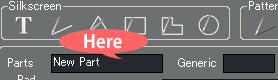
次に部品名を入力します。
下図の場所に
今回は、部品SN74HC541Nのライブラリーを作成しますので、"SN74HC541N”と入力します
(データーシートよりコピーペーストで入力することも可能です)。
総称名を入力します。
下図の場所に
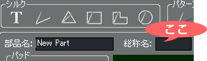
20PIN DIP ですので、"DIP20"と入力します。(データーシートよりコピーペーストで入力することも可能です。)
総称名は入力しなくてもかまいませんが、入力しておくと、部品選択のサーチに使用することができます。
Select [DIP] in the area of [Create Component].
Then the display becomes as follows.
Select [YES].
Next, enter the name of component in the following field.
Enter "SN74HC541N" for creating the library of component, SN74HC541N at this time.
(Entry by copying and pasting from datasheet is available as well.)
Enter the Generic Name in the following field.
Enter "DIP20" because of 20PIN DIP (Entry by copying and pasting from datasheet is available as well).
The entry for this Generic Name is not necessary but this name entered is referred for component selection searching.
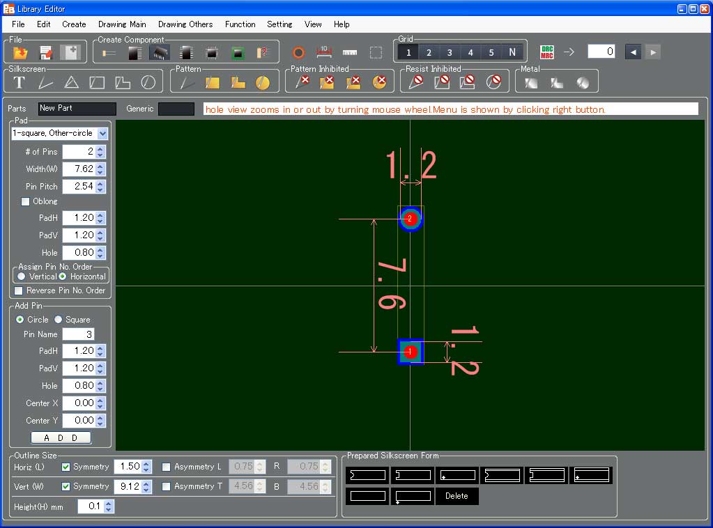
1-3) パッド設定エリアの設定
1-3) Setting Area of Pad
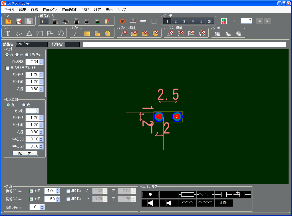
[丸],[角],[1角,他丸]のボタンの中からいずれかを選択し、ライブラリーのパッドの形を決定します。ここでは、[1角,他丸]を選択します。
(ボタンの選択はライブラリーの形を決めるので自由です)
この部品のピン数は20ピンなので、 [Pin数]の設定を”20”にします。
マウスを移動し、直接”20”とキー入力するか、右側のup/down印をマウス左クリックで[20]にします。
[20]にすると下記画面になります。

[縦幅(w)]はデーターシートより7.62(mm) なので、そのままにします。
[Pin間隔]はデーターシートより2.54(mm) なので、そのままにします。
[Pad横(径)]は、Pin幅が、データーシートより0.53mmなので、穴径を0.7mmにします。
Pad径は、最低でも穴径の+0.3mm以上にしなければ、DRCエラーになります
ここでは 0.7mm+0.5mm= 1.2mmなのでそのままにします
[Pad縦]、ここではパットが正円なので、入力の必要は有りません(正円の時はPad横とPad縦は同じになります)。
パットを長円にする場合は、各々の径を入力して下さい。
[穴径]は、先程0.7mmと決めたので”0.7”にします。
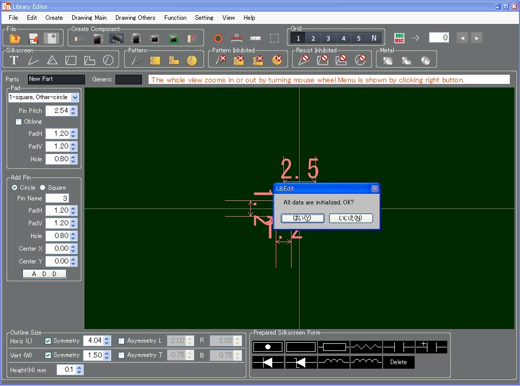
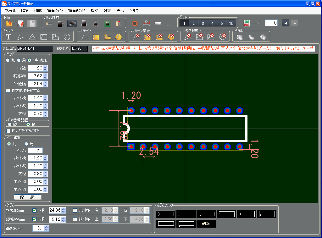
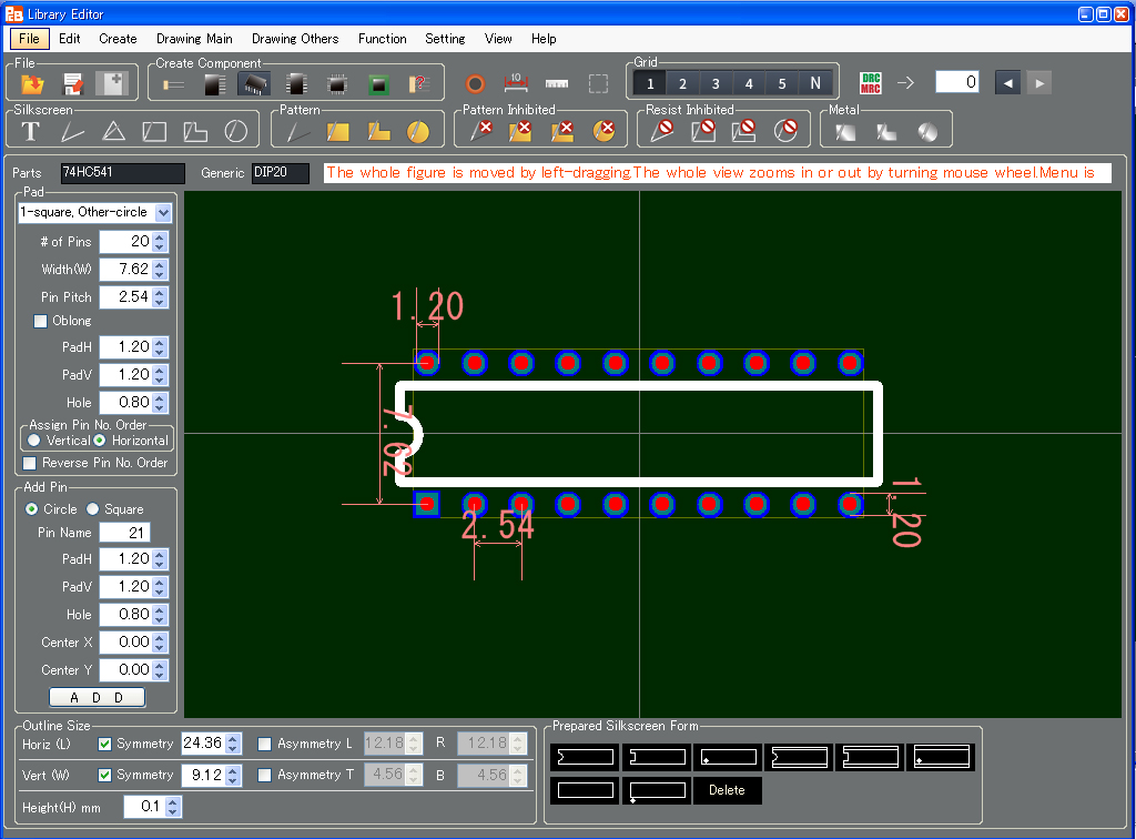
これで基本的なライブラリーができました。
画面は下記のようになります。
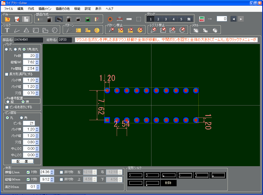
穴径は赤、パットは緑、レジストの逃げは青色で表示されています。
*注1)ピンの周囲のレジストの逃げは自動発生します。特別に必要な場合以外は、入力する必要は有りません。
*注2)ピン追加エリアは、今回追加ピンが無い為、設定の必要はありません。
To select any figure of [Circle], [Square] or [One square, Others circle] decides the pad figure of library. Select [One square, Others circle] for this time.
Set [Number of Pins] "20" because this component's is 20.
Directly enter "20" directly or use up-down button in the right side to be [20].
After setting [20] the view becomes as follows.

Set the [Width(w)] as it is because datasheet's is 7.62(mm).
Set the [Pin Pitch] as it is because datasheet's is 2.54(mm).
Set the [PadH] 0.7mm because datasheet's is 0.53mm.
Unless setting Pad Diamenter (Hole Diameter)+0.3mm or more, DRC error happens.
Here as it is for this time because 0.7mm + 0.5mm = 1.2mm.
No need to enter [PadV] because pads are made perfect circle for this time (In case of perfect circle Pad horizontal is same as Pad vertical).
If setting pads to be long-hole, enter each diameter.
Set [Hole] "0.7" because it is decided as the above.
Then a basic library has been created.
The view becomes as follows.
The color of hole diameter is red, pad's is green and non-resist's is blue.
* Note 1) Non-resist pattern around a pin is generated automatically. No need to enter except for special case.
* Note 2) No need to set items in "Add Pins" because there is no additional pin for this example.
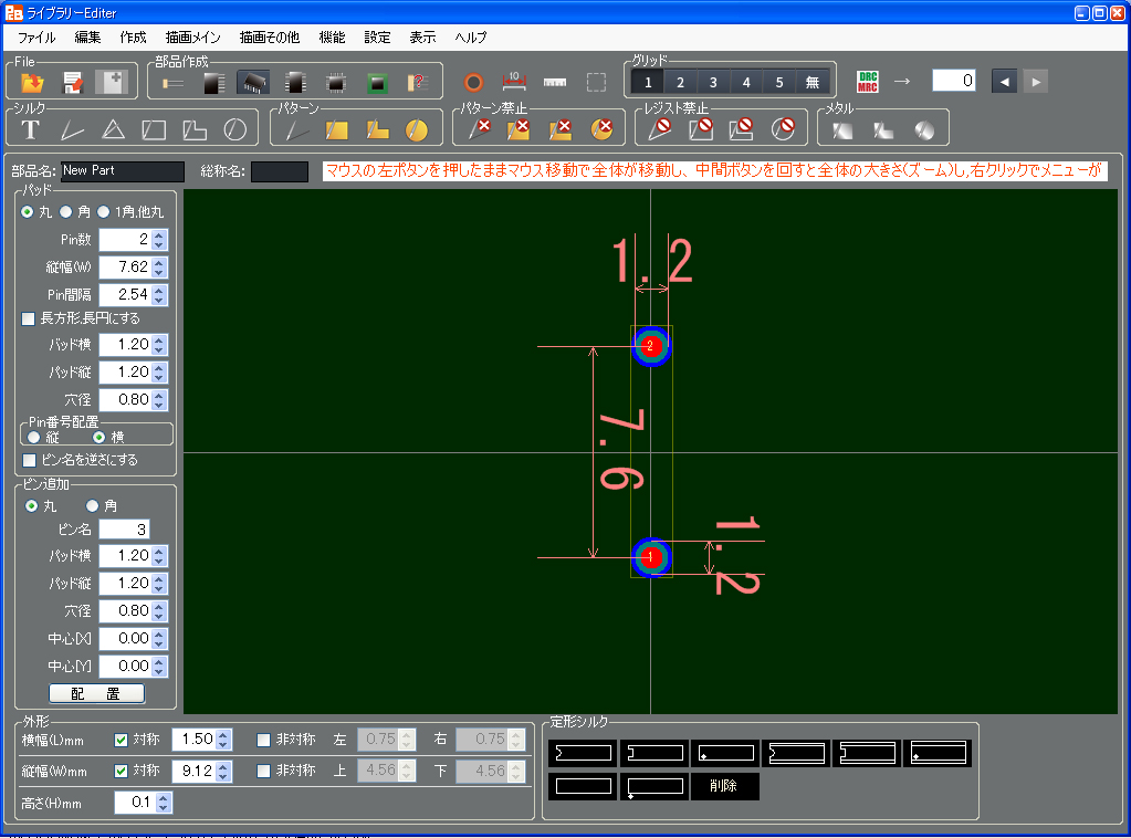
1-4) 外形エリアの設定
1-4) Set the Component Outline
外形はデーターシートより、横幅26.92mm、縦幅7.62mmです。
横幅は左右対象なので、”26.92”と設定します。
縦幅は上下対象で、データーシートより7.62mmですが、7.62mmと設定しても、穴径、パット幅の影響で9.12mmになってしまいますので、そのままにします。
外形は黄色細線で表示されています
*注1)外形は、自動計算された幅よりも小さく設定する事はできません。
部品により、自動計算された幅よりも大きく設定する時のみ設定します。
*2)[非対称]は、データーシートがセンター振り分けで、寸法が記載されていない部品の時に選択します。
The sizes (horizontal and vertical) of the component outline are H:26.92mm and V:7.62mm according to its datasheet.
Set the horizontal width "26.92" because it is horizontally symmetrical.
Although the vertical width is also vertically symmetrical and 7.62mm according to its datasheet, set as it is because it becomes 9.12mm due to the influence of hole diameter and pad width even if setting 7.62mm.
The outline is displayed as yellow sharp line.
* Note 1) The outline size cannot be set less than the value which is automatically calculated for each component.
Set only if being more than auto calculated value.
* Note 2) [Asymmetry] should be selected in case no symmetrical dimension of the component is mentioned in the data sheet.
1-5) シルクの作成
1-5) Create Silkscreen
①[定形シルク]エリアからシルクを選択します。
②[シルク]エリアから[文字][ライン][三角][四角][ポリゴン][円]を使用して作成します。
または、①と②の両方を使用して作成します。
今回は[定形シルク]エリアからシルクを選択します。
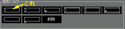
[定形シルク]エリアから上図の場所をクリックします。
すると下図のような表示になり、ライブラリーが完成します。
(1) Select any figure in the area of [Prepared Silkscreen Form].
(2) Use [Character][Line][Triangle][Rectangle][Polygon][Circle] in the area of [Silkscreen].
Use the way of (1) or (2) otherwise, both (1) and (2) for silkscreen's creation.
This time select in the area of [Prepared Silkscreen Form].
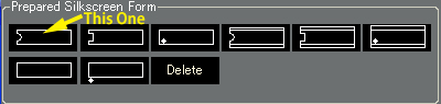
Left-click the arrow's position of the above figure in the area of [Prepared Silkscreen Form].
Then the view becomes as follows and the library is completed.
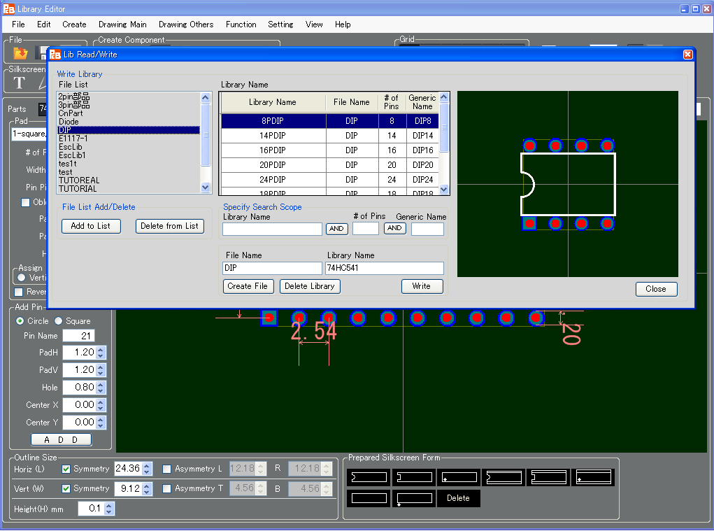
1-6) ライブラリーの書き込み
1-6) Write a Library
ライブラリーをファイルに書き込みます。
[File]エリアから[書込]を選択します。
すると下記画面が表示されます。
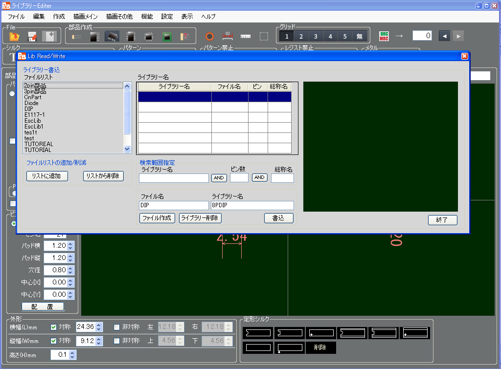
ファイルリストの中から"DIP"を選択(マウス左クリック)します。
すると下記画面に変ります。
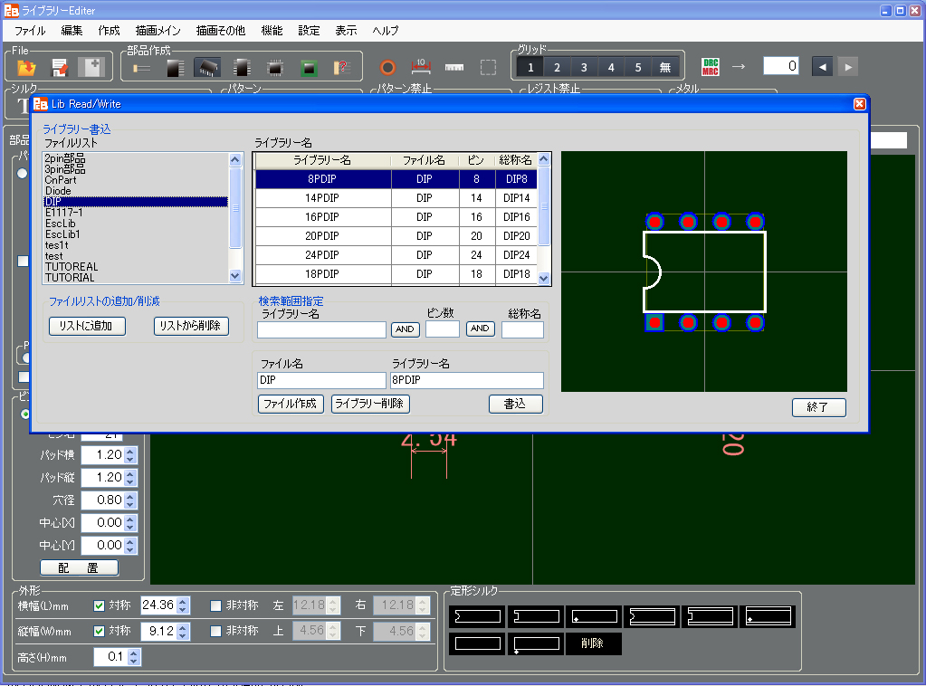
[書込]ボタンを押すと、表示されたライブラリーを書き込みます。
これで1つのライブラリーの作成が終了します。
[終了]ボタンを押し、書き込みを終了します。
再度他のライブラリーを作成する時は、1-2)からの操作を繰り返します。
[ファイル][終了]で、ライブラリーエディターを終了します。
The library is going to be written in the file.
Select [Write] in the menu of [File].
Then the following view is displayed.

Select "DIP" in the File List with left-clicking.
The view is changed as follows.
Pressing the button [Write] writes the displayed library.
The creation of one library is done.
Pressing the button [Close] settles the writing.
If creating another library again, repeat the operation from Chapter 1-2).
Selecting [File][Exit] exits the Library Editor.
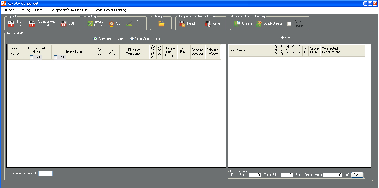
第2章 ネットリスト読み込みとライブラリー読み込み
Chapter 2. Import a Netlist and Open a Library
2-1) ネットリスト読み込み設定
2-1) Setting for importing netlist
2-1-1) ネットリスト読み込み
2-1-1) Import a Netlist
メニュー[ファイル][新規]を選択します。
すると下記画面が表示されます。
[読込、設定]エリアの中から、[ネットリスト]ボタンを押します。
すると下記画面が表示されます。
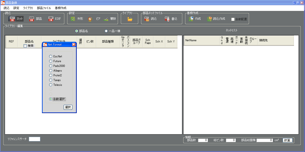
ネットリストフォーマット選択画面が現れます。
今回のネットリストフォーマットは"Pad2000"フォーマットなので [Pad2000]のボタンを押します。
[選択]ポタンを押すと、ファイル選択画面になりますので、"TUTOREAL1.net"を選択し[開く]ボタンを押して下さい。
すると下記画面が表示されます。
Select Menu > [File] > [New].
Then the following view appears.
Press the button [NetList] in the area of [Import].
Then the following appears.
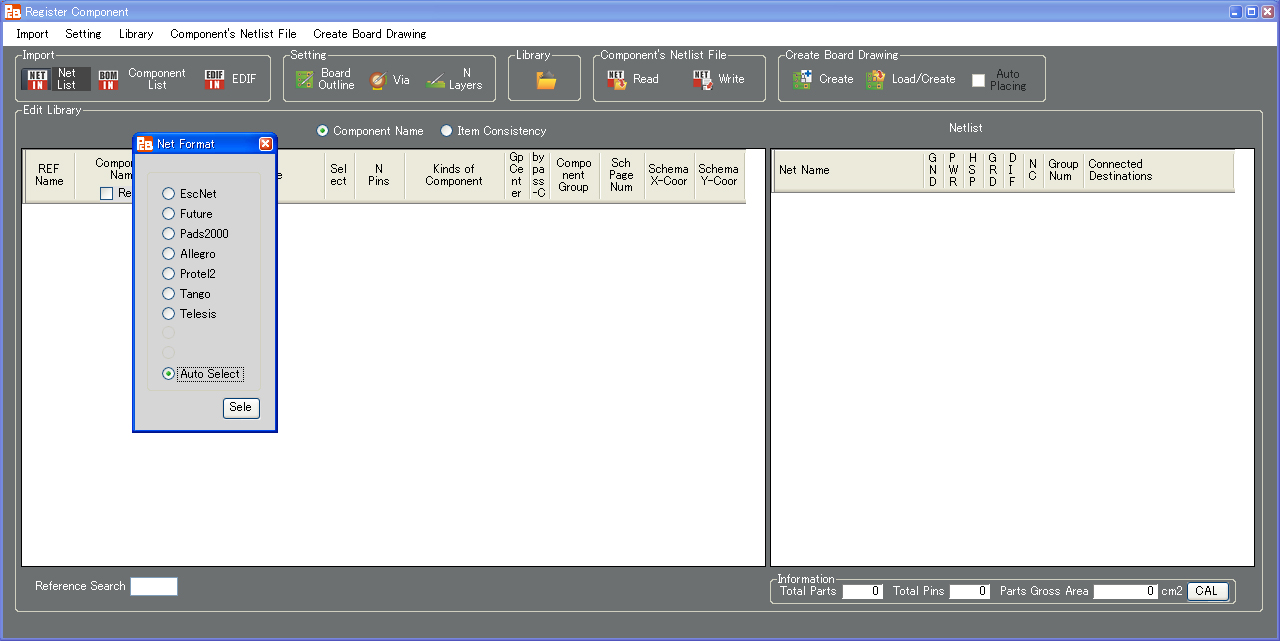
The window of selecting netlist format is opened.
Press the button [Pads2000] because of "Pads2000" format for this time.
Selecting the button [SEL] opens the window of selecting file then choose "TUTOREAL1.net" and press the button [Open].
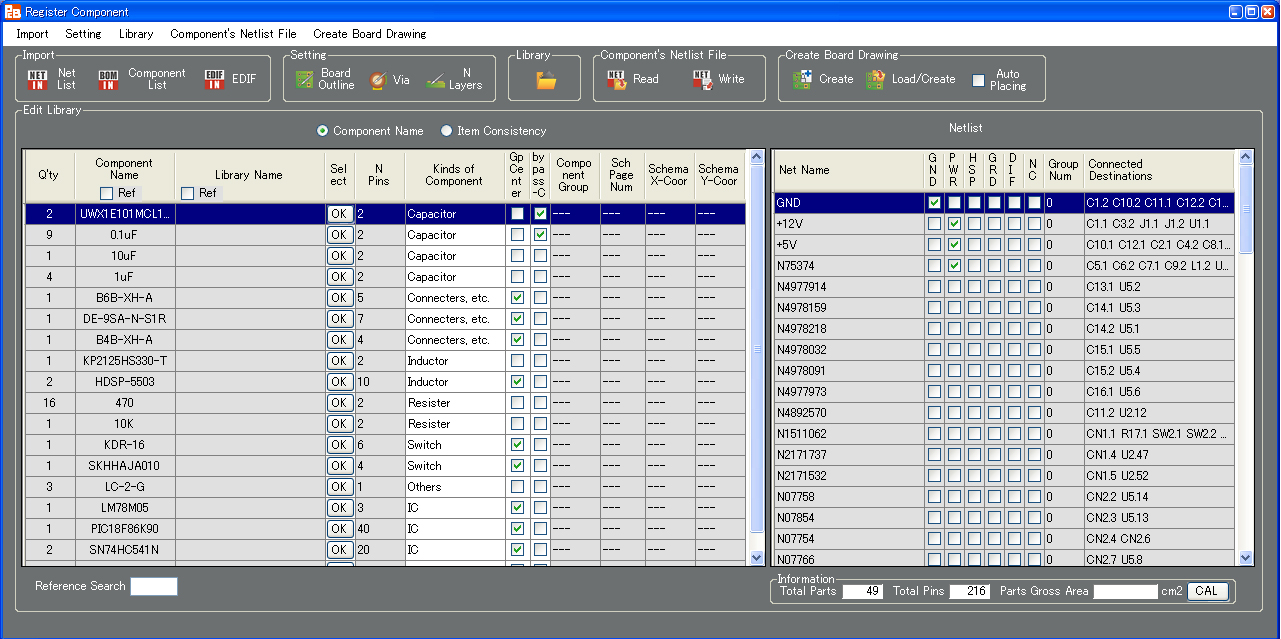
Then the view becomes as follows.
2-1-2) 部品表を入力する(今回は未入力にします)
2-1-2) Entry in a component list (although no entry for this time)
[読込、設定]エリアの中から、[部品表]を選択します。
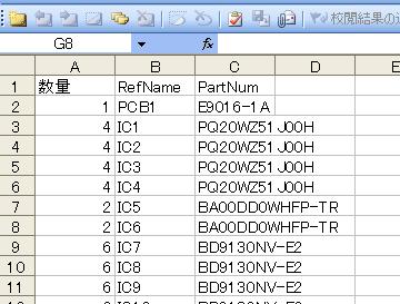
部品表はエクセル"csv"ファイルで、下記フォーマットの部品表のみ受け付けます。
部品表を入力すると[ライブラリー編集]画面の[部品名]の欄が、部品表の部品名に変わります。
Select [Component List] in the area of [Import].
The file type of a component list should be ".csv" and only the component list of the following format can be acceptable.
Once entering in the component list, the column of [Component Name] in the view of [Edit Library] is changed to the component name of the component list.
2-1-3) EDIFファイルを入力する(今回は未入力にします)
2-1-3) Import an EDIF file (although no import for this time)
[読込、設定]エリアの中から、[EDIF]を選択します
EDIFファイルは、ORCAD VER16.5 以上の”Export Design”で出力される EDIF ファイルのみ入力可能です。
(EDIF ファイルを入力すると、自動的に部品グループを形成します。)
Select [EDIF] in the area of [Import].
The EDIF file should only be exported with ORCAD version 16.5 or more by "Export Design"
(Once importing an EDIF file, component group is created automatically.)
2-1-4) 基板外形入力
2-1-4) Entry of Board Outline
[読込、設定]エリアの中から、[基板外形]を選択します
すると下記画面が表示されます。
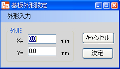
基板の最大外形寸法を入力します。
今回は、取りあえずX=100mm Y=100mm に設定します。
(外形寸法は設計中にも、簡単に修正する事ができます。)
[決定]ポタンを押し、外形寸法入力を終わります。
Select [Board Outline] in the area of [Setting].
Then the following view appears.
Enter the maximum dimension of board outline.
Set X=100mm and Y=100mm for the present.
(It can also be changed easily even during designing.)
Pressing the button [SET] settles the entry of the outline size.
2-1-5) ビア設定
2-1-5) Setting for Via
[読込、設定]エリアの中から、[ビア設定]を選択します
すると下記画面が表示されます。
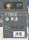
今回は貫通ビアなので、そのまま[決定]ポタンを押します。
(ビア設定は設計中にも、簡単に修正する事ができます)
Select [Via] in the area of [Setting].
Then the following view appears.
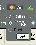
Press the button [SET] without any changes because of through-hole via for this time.
(It can also be changed easily even during designing.)
2-1-6) 層数
2-1-6) The Number of Layers
[読込、設定]エリアの中から、[層数]を選択します
すると下記画面が表示されます。
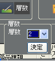
今回は4層基板で設計しますので [4]を選択します。
(層数は設計中にも、簡単に修正する事ができます)
[決定]ポタンを押し、層数入力を終わります。
Select [N Layers] in the area of [Setting].
Then the following view appears.
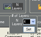
Select [4] because of designing in four layers for this time.
(It can also be changed easily even during designing.)
Pressing the button [SET] settles the entry of the number of layers.
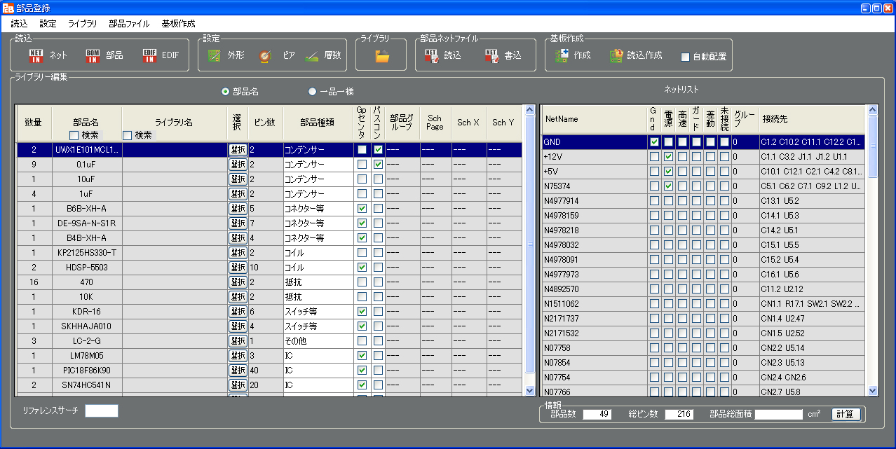
2-2) ライブラリー部品の選択
2-2) Select Library Component
●[ライブラリー編集]エリアの[部品名]ボタン , [一品一様]ポタンの解説
これからライブラリー部品の選択を行いますが、[部品名]ボタンを選択している場合は、同じ部品名の全ての部品にライブラリーの選択を行います。[一品一様] ボタンを選択している場合は、1つの部品にそれぞれ1つづつライブラリーの選択を行います。
同じ部品でも違うライブラリーを選択したい場合は、最初に[部品名]ボタンを押し同一のライブラリーを選択してから、[一品一様]ボタンを押し違うライブラリーのみ再選択すると効率が良いでしょう。
再度[部品名]ボタンを押すと、従来のライブラリーに加えて、新たに選択したライブラリーも表示されます。
●Explanation of the button [Component Name] and [Item Consistency] in the [Edit Library] area
From here a library component is going to be selected. In case the button [Component Name] has been selected, the library selection will be done in all the components which are same component name. In case the button [Item Consistency] has been selected, one library will be selected in one component.
If selecting a different library even for the same component, it could be efficient to press the button [Component Name] and select the same libraries at first then press the button [Item Consistency] and select again just the different libraries.
Pressing the button [Component Name] again displays newly selected library in addition to the existed library as well.
2-2-1) 選択方法
2-2-1) Selection Method
[ライブラリー編集]エリアで、選択したい部品の行の[選択] ボタンを押します。
すると下記画面が表示されます。
全てのライブラリーリストから、選択したい部品のピン数と一致するライブラリーのみが表示されます。
表示されたライブラリーリストから、ライブラリー名を[↑][↓]キーでスクロールすると該当する図形が右側に表示されます。
その中から、ダブルクリックするか、[選択]ボタンを押して、必要なライブラリー名を決定します。
[検索範囲指定]エリアで、[ライブラリー名]欄に検索したい文字を入力すると、その文字を含んでいるライブラリー名のみをライブラリーリストに表示します。
加えて、[ピン数]・[総称名]欄に、検索したいピン数、文字を入力すると、より絞り込んだ検索をする事ができます。
部品のピン数とライブラリーのピン数が一致しない時は、ピン数を空白にするか、別のピン数を入力し、必要なライブラリーを探します
今回の回路で必要なライブラリーは、ファイルリストの"TUTORIAL"に全て含まれていますので、ファイルリストの"TUTORIAL"を選択すると探し易いでしょう
ここまでで、取りあえず現在の画面は、[閉じる]で表示を消します。
Press the button [OK] of the line (row) of which the component should be selected in the [Edit Library] area.
Then the following view appears.
Only the library of which the number of pins matches with the one of component which should be selected in all the library lists is shown.
Scrolling for selecting a library name in the Library List with the keys [↑] or [↓] shows the component figure of the selected one in the right frame.
Left-double-clicking any of them or pressing the button [Select] decides the intended library name.
If entering characters in the field [Library Name] in the area of [Specify Search Scope] to be searched, just the library names which include such characters are listed in the Library List.
In addition, if entering the number of pins and characters in the fields [# of Pins] and [Generic Name] to be searched, more selective searching can be done.
In case the number of the component is not matched with the one of the library, empty the number of pins or enter another number of pins for searching the intended library.
All the libraries which are necessary for this tutorial's circuit are included in "TUTORIAL" in the File List which should be selected for searching easily.
Press the button [Close] for closing the present window temporarily.
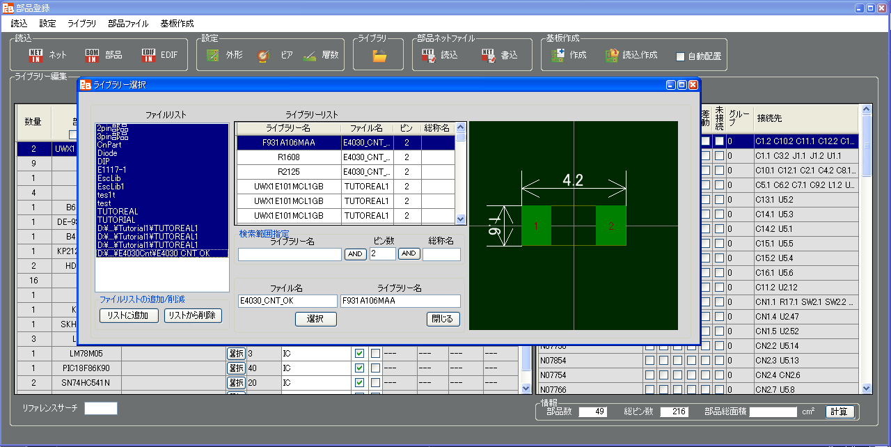
2-2-2) ライブラリー選択の実際
2-2-2) Do Selection of Actual Library
[ライブラリー編集]エリアの部品名"UWX1E101MCL1GB" を選択してみましょう。
部品名"UWX1E101MCL1GB"と同じ行の[選択]ボタンを押すと、[ライブラリー選択]画面が表示されます。
ファイルリストから"TUTORIAL"を選択すると、"TUTORIAL"の中に入っている、ライブラリーの2ピン部品のみ表示されます。
ライブラリーリストを選択し、[↑][↓]キー又はライブラリーリスト右の上下バーで、ライブラリー名"UWX1E101MCL1GB"を選択し、[選択]ボタンを押すか、ダブルクリックします。
次に部品名 "0.1uF" の部品を選択します。
前回の選択時同様、同じ行の[選択]ボタンを押します。
ファイルリストから"TUTORIAL"を選択します。
ライブラリーリストから"C2125"を選択し、[選択] ボタンを押します。
次に、部品名 "10uF" の部品を選択します。この部品も"C2125"になりますので、0.1uF" の[ライブラリー名]列を左クリックし、"コントロールキー"+"C"を押します。次に"10uF"の行の[ライブラリー名]列を左クリックし、"コントロールキー"+"V"を押します。すると[ライブラリー名]列が空白から"C2125"に変わります。
このように[ライブラリー名]列はコピー&ペーストが可能です。
次に、部品名 "1uF" の部品を選択します。
この部品も"C2125"になるので、"1uF"の行の[ライブラリー名]列を左クリックし、"コントロールキー"+"V"を押します。するとここでも[ライブラリー名]列が空白から"C2125"に変わります。
次に部品名 "B6B-XH-AM" の部品を選択します。
ファイルリストから"TUTORIAL"を選択すると、"TUTORIAL"の中に入っているライブラリーの5ピン部品のみ表示されます。
"B6B-XH-AM"は、実際には6ピン部品ですので、このライブラリーリストには"B6B-XH-AM"は載っていません。
{ネットリストでは、実際に使用されているピン(回路図で空きピンになっていないピン)のみを抽出するため、ここでは5ピン部品となってしまうためです}
[検索範囲指定]エリアの[ピン数]欄を"6"に修正して下さい
そうすると6ピン部品が表示され、"B6B-XH-AM"がライブラリーリストに表示されます。
ライブラリーリストを選択し、[↑][↓]キー又はライブラリーリスト右の上下バーで
ライブラリー名"B6B-XH-AM"を選択し、[選択]ボタンを押すか、ダブルクリックします。
上記の操作を繰り返し、全ての[ライブラリー名]列を埋めていきます。
Let's select the component name "UWX1E101MCL1GB" in the [Edit Library] area.
Press the button [OK] in the same line (row) as the component name "UWX1E101MCL1GB" then the view of [Library Selection] appears.
Select "TUTORIAL" in the file list then only two pins component of the library in the "TUTORIAL" folder is shown.
Select the library list then select the library name "UWX1E101MCL1GB" with the keys [↑][↓] or slide bar then press the button [OK] or left-double-click it.
Next is the selection of the component named "0.1uF".
Press the button [OK] in the same line (row) as with the previous selection.
Select "TUTORIAL" in the file list.
Select "C2125" in the library list then press the button [OK].
Next is the selection of the component named "10uF". Because the name of this component is "C2125", left-click the column of [Library Name] of "0.1uF" line (row) then press the keys "CTRL"+"C". Then left-click the column of [Library Name] of "10uF" line (row) and press the keys "CTRL"+"V". Finally, the contents of the column [Library Name] change from empty to "C2125".
Thus, the contents in the column [Library Name] can be copied and pasted.
Next is the selection of the component named "1uF".
Because it is also "C2125", left-click the cell of row "1uF" and column [Library Name] and press the keys "CTRL"+"V". Finally, the cell of column [Library Name] also changes from empty to "C2125".
Next is the selection of the component named "B6B-XH-AM".
Select "TUTORIAL" in the file list then just five-pins component of the library in the folder "TUTORIAL" is listed.
Because "B6B-XH-AM" is actually six-pins component, no "B6B-XH-AM" is listed in this library list.
{Because just the actually used pins (no open-pins in the circuit diagram) are abstracted in the netlist, the number of the pins of such component is recognized to be five.}
Change to "6" in the field [# of Pins] in the area of [Specify Search Scope].
Then the components of six pins including "B6B-XH-AM" are listed in the Library List.
Focus in the Library List then
select the library name "B6B-XH-AM" with the keys [↑][↓] or the right slide bar then press the button [Select] or left-double-click it.
Repeat the abovementioned operations for filling in all the fields of the column of [Library Name].
2-2-3) 部品種別
2-2-3) Component Type
部品種別は、部品のリファレンス名、ピン数などのデーターにより、自動で設定されます。
そのため、部品"HDSP-5503"のように、部品種別が違っている場合が有ります。
部品種別を修正する場合は、修正したい場所でマウスを左クリックし、種別選択します。
部品種別は、基板設計には使用されませんが、部品グループ化の時に使用します。
Component type is automatically judged and set by the data such as reference name or the number of pins of the component.
So that there is a case of wrong component type such as the component "HDSP-5503".
If changing a component type, left-click the position where the change should be done and select a type.
This component type is not used for designing board but is used for grouping components.
2-2-4) GPセンタ
2-2-4) Group Center (GP Center)
GPセンタとは、部品グループ化の時に、グループの中心部品になる部品です。
GPセンタは、部品のリファレンス名、ピン数、部品種別などのデーターにより、自動で設定されます。
修正することは可能ですが、ここでは修正しません。
"GP Center" means the component which would become the center component of the group for grouping components.
It is automatically judged and set by the data such as reference name, the number of pins or component type.
It can be changed but is not done now.
2-2-5) パスコン
2-2-5) Bypass Capacitor
パスコンは、部品のリファレンス名、ピン数、接続先などのデーターにより、自動で設定されます。
修正することは可能ですが、ここでは修正しません。
Bypass capacitor is judged and set by the data such as reference name, the number of pins or its destination.
It can be changed but is not done now.
2-3) 部品のグループ化
2-3) Grouping Components
部品のグループ化を設定しておくと、部品の配置を容易に実行することができます。
(グループ配置は、大変便利な機能ですので、部品のグループ化は、ぜひ設定して下さい)
また2-1-3)でEDIFの読み込みをした場合は、自動で設定されます。
回路図を見ながらの作業になりますので、回路図を手元に置いてください。
[ライブラリー編集]エリアの[一品一様]ポタンを押して下さい。
[部品グループ]列で白い部分が選択可能です。
まずこの部分をマウスクリックし選択すると、選択部品一覧(GPセンタの一覧)が表示されますので、さらにその中から選択します。
リファレンス [C1]、部品名 [UWX1E101MCL1GB] の部品グループの部品(GPセンタ)を選択してみましょう。
回路図を見ると、[C1]は[U1]の部品名[LM78M05]の近くにありますので、選択部品一覧の中から"U1"を選択します。
リファレンス [C2]、 部品名 [UWX1E101MCL1GB] の部品グループの部品(GPセンタ)を選択してみましょう。
回路図を見ると、[C2]は[U1]の部品名[LM78M05]の近くにありますので、選択部品一覧の中から"U1"を選択します。
リファレンス [C3] 、部品名 [0.1uF] の部品グループの部品(GPセンタ)を選択してみましょう。
回路図を見ると、[C3]は[U1]の部品名[LM78M05]の近くにありますので、選択部品一覧の中から"U1"を選択します。
リファレンス [C4] 部品名 [0.1uF] の部品グループの部品(GPセンタ)を選択してみましょう。
回路図を見ると、[C4]は[U1]の部品名[LM78M05]の近くにありますので、選択部品一覧の中から"U1"を選択します。
リファレンス [C5]、 部品名 [0.1uF] の部品グループの部品(GPセンタ)を選択してみましょう。
回路図を見ると、[C5]は[U2]の部品名[PIC18F87K90]の近くにありますので、選択部品一覧の中から"U2"を選択します。
以下このように設定していきます。
A placing components can easily be executed if setting grouping components in advance.
(This function is very useful, therefore we strongly suggest you do it.)
Also, in case of reading EDIF file mentioned in chapter 2-1-3), it is automatically set.
Put the circuit diagram at hand because the following procedure needs to look at it.
Select [Item Consistency] in the [Edit Library] area.
The white parts in the column [Component Group] are selectable.
Left-click this part for selection first, then the list of selected components ("GP Center") is shown and select in the list continuously.
Let's select the component (GP Center) of component group of reference [C1] / component name [UWX1E101MCL1GB].
Because the circuit diagram shows that [C1] is near the component name [LM78M05] of [U1], select "U1" in the selected component list.
Let's select the component (GP Center) of component group of reference [C2] / component name [UWX1E101MCL1GB].
Because the circuit diagram shows that [C2] is near the component name [LM78M05] of [U1], select "U1" in the selected component list.
Let's select the component (GP Center) of component group of reference [C3] / component name [0.1uF].
Because the circuit diagram shows that [C3] is near the component name [LM78M05] of [U1], select "U1" in the selected component list.
Let's select the component (GP Center) of component group of reference [C4] / component name [0.1uF].
Because the circuit diagram shows that [C4] is near the component name [LM78M05] of [U1], select "U1" in the selected component list.
Let's select the component (GP Center) of component group of reference [C5] / component name [0.1uF].
Because the circuit diagram shows that [C5] is near the component name [PIC18F87K90] of [U2], select "U2" in the selected component list.
Continue to set according to the abovementioned.
2-4) ファイルのセーブ
2-4) Save File
[部品,ネットセーブ]ボタンを押すと、ここまでのファイルを一旦保存します。
[部品,ネットセーブ]ボタンを押します。
すると下記画面が表示されます。
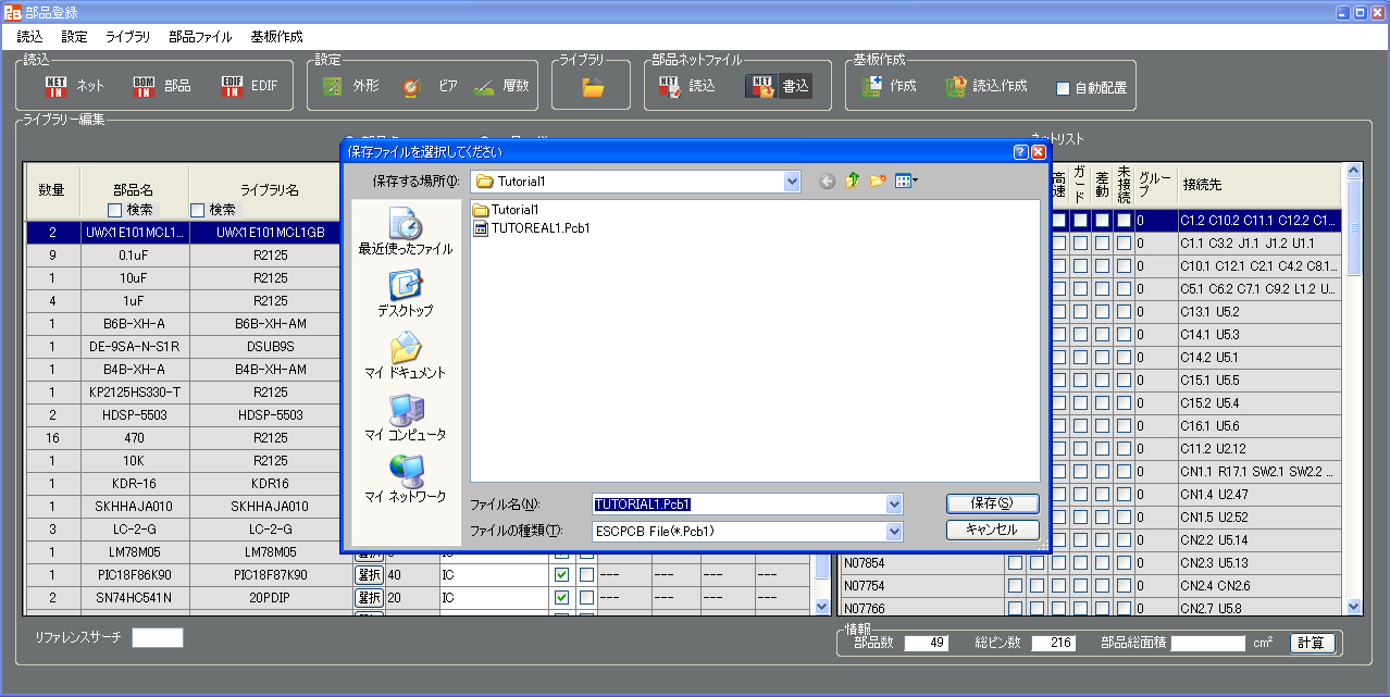
セーブする時はファイル名が必要です。"Trutorial1.pcb1"はすでに有りますので、ここでは、別の名前にして下さい。
(Trutorial1.pcb1"は予め作成したデーターです)
To press the button [Write] saves the present file temporarily.
Press the button [Write].
Then the following view appears.
Entry of a file name is necessary for saving. Because the name "Trutorial1.pcb1" has already been existed, enter another name here.
("Trutorial1.pcb1" has been created in advance.)
2-5) ネットリストエリア
2-5) NetList Area
[ライブラリー編集]->[ネットリスト]
このエリアはこのバージョンでは使用しませんので、そのままにします。
これで全てのライブラリー登録ができましたので、次に進みます。
[Edit Library]->[Netlist]
This area is not used and is left unchanged for this case (version).
Go forward because all the library registrations have been done.
2-6) [基板作成]ボタン
2-6) Button [Create]
[基板作成]ボタンを押します。
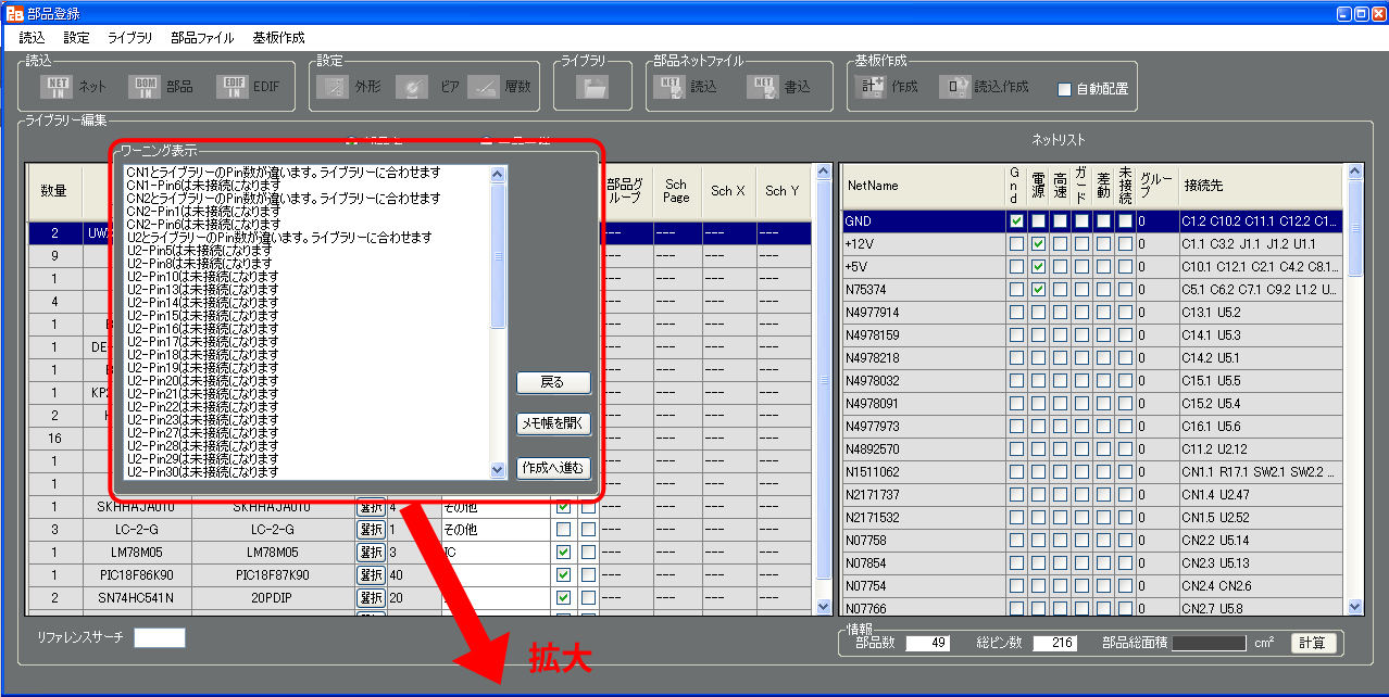
すると下記のように[ワーニング表示]が表示されます。
Press the button [Create].
Then the following [Warning Announce] is displayed.
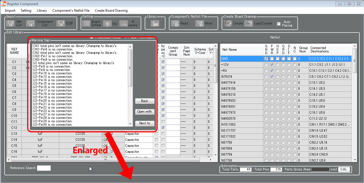
拡大図
Enlarged Figure
メッセージは2種類あります。
①"CN1とライブラリーのPin数が違います。ライブラリーに合わせます"
このメッセージは、ネットリストから抽出した部品のピン数と、選択したライブラリーのピン数が合っていない場合です。
例えばここでは、[CN1]の部品名"B6B-XH-AM"にこのメッセージが出ていますが、部品選択の時ピン数が合っていませんでしたので{2-2-2)参照}、問題は有りません。
②"CN1-Pin6は未接続になります"
このメッセージは、ライブラリーには存在していますが、ネットリストには存在していないピンの表示です。
例えばここでは、回路図を見ると"CN1-6"は未接続ですから、問題は有りません
ここで注意する点は、回路図では接続されているピンに、このメッセージが出た場合です。
この場合は、ネットリストが違うか、ライブラリー選択で間違ったライブラリーを選択した可能性が有ります。
そのような場合は[戻る]ボタンを押し、それぞれに必要な修正をして下さい。
メッセージの確認が終わったら、[作成へ進む]ボタンを押して下さい。
[部品登録]画面が消えて、メイン画面になります。
There are two kinds of messages.
(1)"CN1 total pins isn't same as library. Changing to library's."
This message appears in case the number of pins of the component which is acquired from the netlist is not matched with the one of the selected library.
For instance this message appears here in the component name "B6B-XH-AM" of [CN1] however, it is no problem because the numbers of pins have not been matched at selecting component (refer to chapter 2-2-2)).
(2)"CN1-Pin6 is no connection."
This message appears in case it is existed in the library but not in the netlist.
For instance, here is no problem because "CN1-6" is not connected with any destination in the circuit diagram.
Be careful here if this message appears in the pin which is connected with any destination in the circuit diagram.
In this case the netlist may be different or a wrong library might be selected at the library selection.
In such situation press the button [Back] then correct properly.
After the message confirmed, press the button [Next to].
The [Register Component] window disappears then the view returns to the main window.
2-7) [ロード&基板作成]ボタン
2-7) Button [Load/Create]
[部品,ネットロード]ポタン+[基板作成]ボタンと同じ機能です。
This function is same as the one of buttons [Read] & [Create].
第3章 取り付け穴を付ける
Chapter 3. Create Mounting Hole
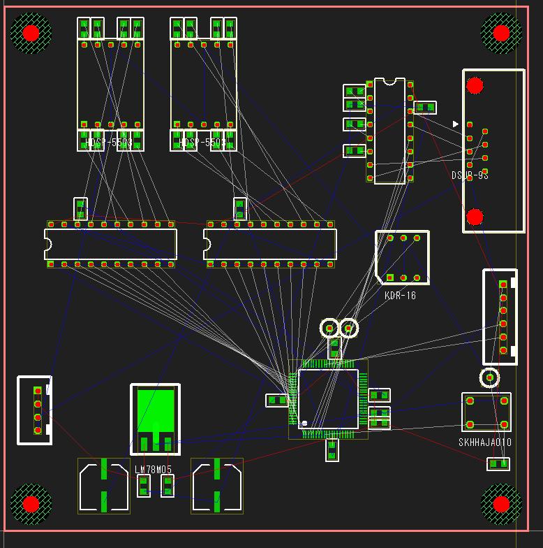
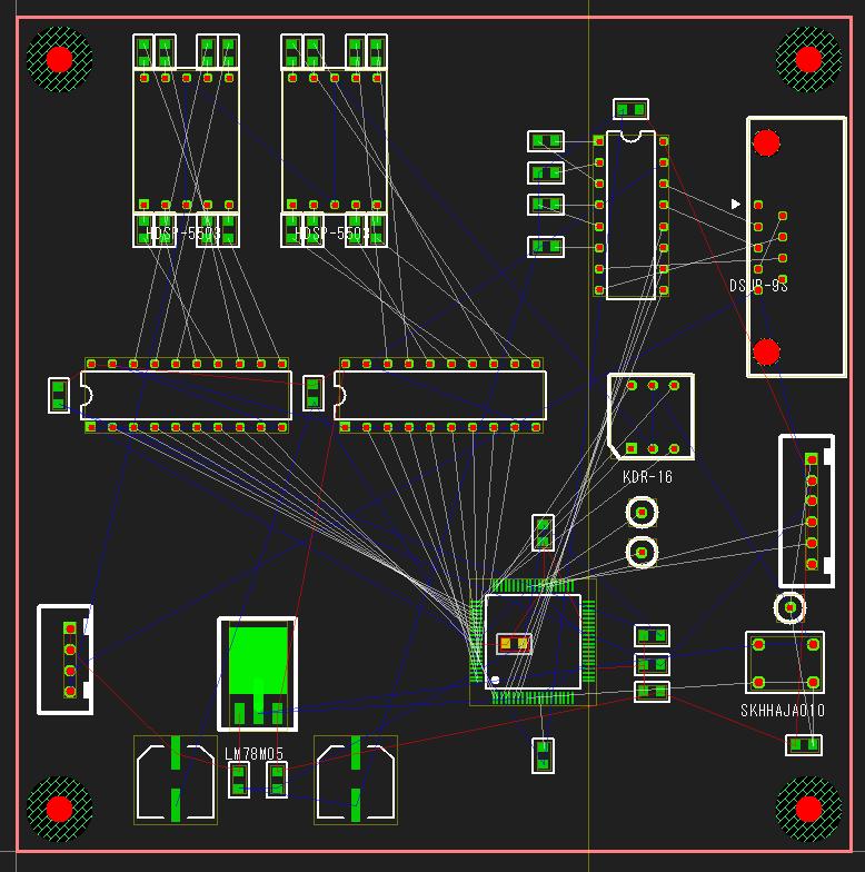
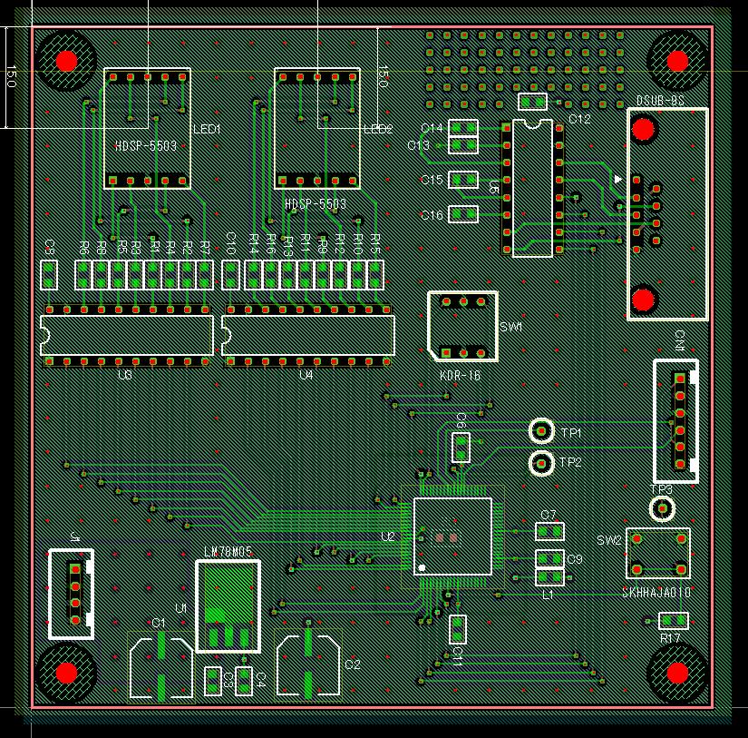
メイン画面に、いまだ未配置の部品が表示されています。
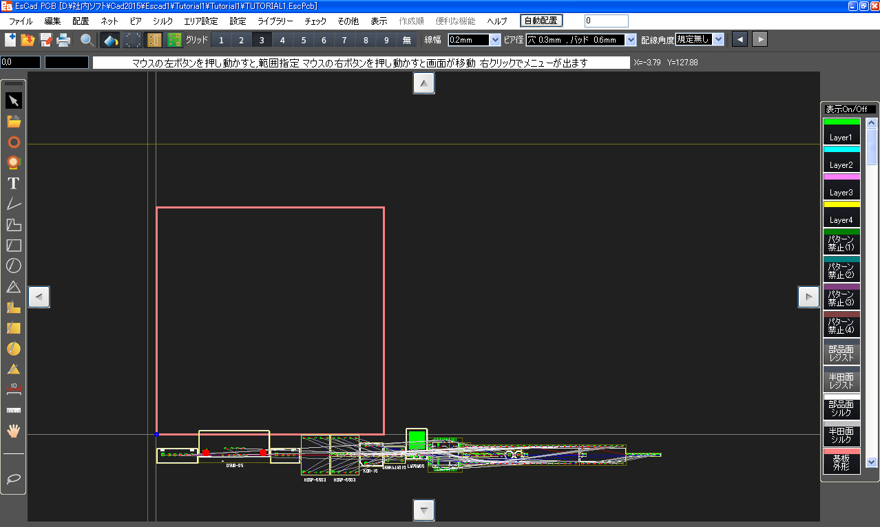
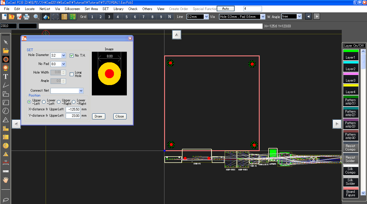
基板の四隅5mmの位置に、4箇所、取り付け穴を取り付けます。
まず[グリッド]エリアの[9]のボタンを押すと、グリッドが5mmに設定されます。
次に、メニュー[設定]->[取付穴作成]を選択すると、[取付穴]画面が表示されます。
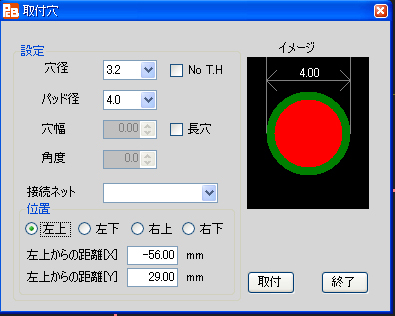
ここでは、穴径を”3.2”mm にし、[No. T.H] にチェックを入れます。さらに禁止径を”8”mm に設定します。
位置指定での取り付けも可能ですが、今回はマウスの移動と画面の拡大・縮小を用いての取り付けを行います。
取り付け穴を設定したい場所に、マウスを移動します。
移動すると、赤円の取り付け穴のイメージがマウスと共に移動します。
取り付けたい位置が表示範囲外の場合は、マウスの中心を回すと、画面が拡大・縮小しますので、一旦画面を縮小して、取り付けたい位置を取りあえず表示させます。表示された取り付け位置にマウスを移動し、再度画面を拡大して取り付け位置を設定します。
また[↑][↓][→][←]キーを押す事により、位置を移動する事ができます。
設定位置でマウスを左クリックすると、取り付け穴を1つ設定できます。
残り3箇所も同じ要領で設定します。
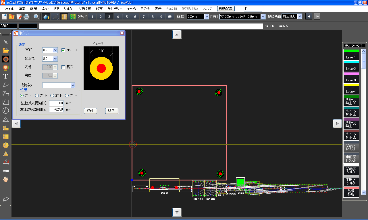
取り付け穴4箇所の設定が終了したら、[取付穴]画面の[終了]ボタンを押します。
The main window shows components which are not placed yet.
Four mounting holes at the positions spaced out 5mm from the (four) corners of the board are created..
First, press the button [9] in the [Grid] area then the display grid width is set 5mm.
Next, select Menu [SET]->[Create Mounting Hole] then the form of [Mounting Hole] is opened.
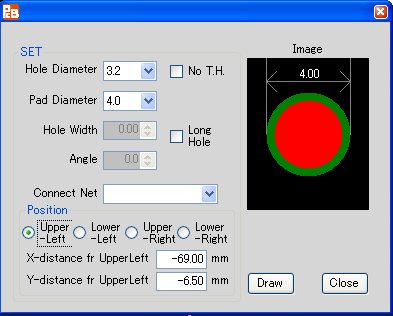
Now, Set the hole diameter "3.2"mm and do checked [No. T.H] on. Moreover set the [No Pad] "8"mm.
For this case those are going to be placed with mouse operation and zooming up and down as follows even though it can be done with specifying the location value.
Move a cursor to the position where the mounting hole should be placed.
Moving a cursor moves the mounting hole's image of red circle together.
If such position is out of the view of the Drawing Area, rotate the mouse's wheel to zoom the view down then display such position anyway. Move a cursor to such position, rotate the wheel to zoom the view up and display the precise position.
Pressing the keys [↑][↓][→][←] can move the view of the Drawing Area.
Left-click the intended position then one mounting hole can complete to be set.
Do the similar way for other three positions.
After four mounting holes has completed to be set, press the button [Close] in the [Mounting Hole] window.
第4章 配置
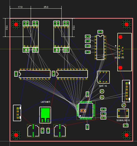
Chapter 4. Component Placement
4-1) グループ配置
4-1) Place Component Group
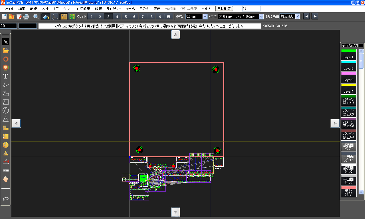
メニュー[配置] ->[グループ配置(片面)]を選択します。
下記画面のように、グループ化した部品が部品(GPセンタ)の周辺に集合しています。
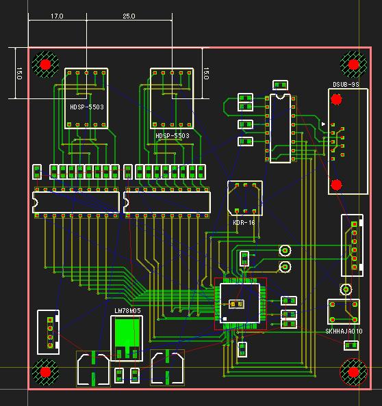
(ここまでのパターン図はTUTORIAL1_1.EscPcbになります)
Select Menu [Placement] ->[Group Placement (One Side)].
Then the grouped components gather around the "GP Center" as the following figure.
(The pattern data up to here is TUTORIAL1_1.EscPcb.)
4-2) 部品移動
4-2) Move Component
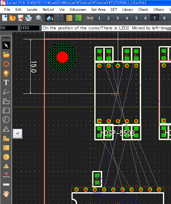
ここでは、[LED1]を左上に移動する手順を説明します。
[グリッド]エリアのボタン[7]を押し、グリッドを1.27mmにします。
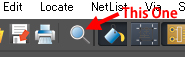
[部品サーチボタン]を押し、[LED1]を探します。
[部品検索]画面が表示されますので、上の入力枠に"LED1"と入力し、エンターキーを押します
すると[部品検索]画面が消え、部品[LED1]の中心上に赤丸が点滅し消えます。
また部品[LED1]が選択状態になります。
[LED1]が見つかりましたので、[LED1]を基板上の左上に移動します。
[LED1]の中心あたりにマウスを移動し、シフトキーを押しながら、
マウス左ボタンを押しながらマウスを移動します。
すると[LED1]とそのグループ部品が一緒に移動します。
このように、GPセンタ部品を、シフトキーを押しながら移動すると、グループ移動ができます。
また、シフトキーを押しながら、[R]キーを押すとグループで回転します。
(シフトキーを押さないと、単体移動または単体回転になります。)
(GPセンタ部品以外では、シフトキーを押しても、単体移動または単体回転になります。)
このように、GPセンタ部品のみ配置していくと、大雑把な配置が完了します。
(ここまでのパターン図はTUTORIAL1_2.EscPcbになります)
ここからは、グループ毎に、GPセンタ部品以外を適切な位置に配置します。
この場合は、シフトキーを押さずに、単体で移動させていきます。

(ここまでのパターン図はTUTORIAL1_3.EscPcbになります)
[C5]は裏面に配置をします。
[C5]を[U2]中に移動します。
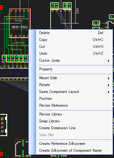
[U2]の上にマウスを置き、マウスを右クリックしメニューを出します。
すると下記画面になります。
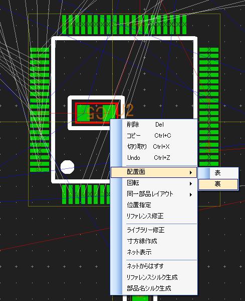
メニューの中から[配置面]→[裏]を選択します。
[C5]のパッドの色が緑から黄色に変りました。
これにより、[C5]が裏面(レイヤー4)に配置されました。
The followings are procedures for the component [LED1] to be moved to the upper-left.
Press the button [7] in the [Grid] area for setting the grid width 1.27mm.
Press the button [Reference Search] for finding [LED1].
The [Search Component] form is opened then enter "LED1" in the above field and press the ENTER key.
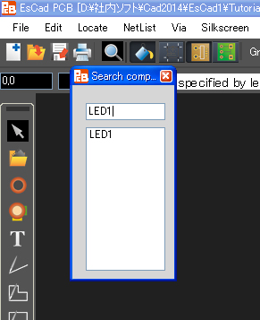
Then the [Search Component] form is closed and the red dot appears and flashes on the center of the component [LED1].
Also, the component [LED1] becomes under selected.
Because the component [LED1] has been found, [LED1] is moved to the upper-left in the board as follows.
Move the cursor around the center of [LED1] and left-drag with pressing the key SHIFT.
Then [LED1] and its grouped components are moved together.
Thus, left-dragging the "GP Center" component with pressing the key [SHIFT] can move the component group.
Also, pressing the key [R] with pressing the key [SHIFT] rotates the component group.
(If with pressing no key [SHIFT], it moves or rotates each component, not group.)
(In case not "GP Center" component, even if with pressing the key [SHIFT], it moves or rotates each component.)
Thus, continue to place just "GP Center" components then rough placement is completed.

(The pattern data up to here is TUTORIAL1_2.EscPcb.)
From here components except "GP Center" in each group are going to be placed at the appropriate position.
In this case go to move a component alone without pressing the key [SHIFT].
(The pattern data up to here is TUTORIAL1_3.EscPcb.)
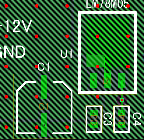
Place the component [C5] at the back side.
Move [C5] in the [U2].
Move a cursor on the [U2] then right-click for opening popup-menu.
Then the view becomes as follows.
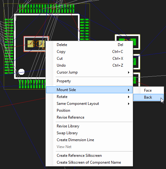
Select [Placement Side]→[Back] in the menu.
The color of [C5]'s pad has changed from green to yellow.
That means [C5] has been placed at the back side (Layer 4).
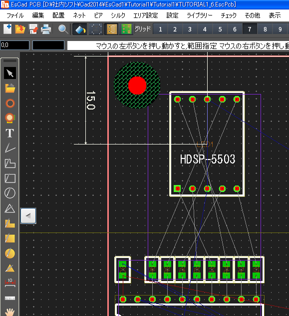
4-3) 位置指定
4-3) Specify Position
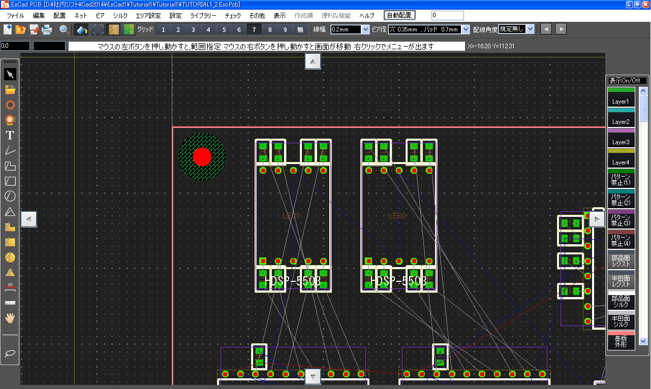
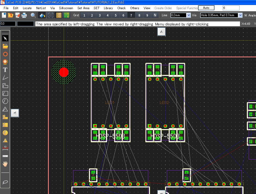
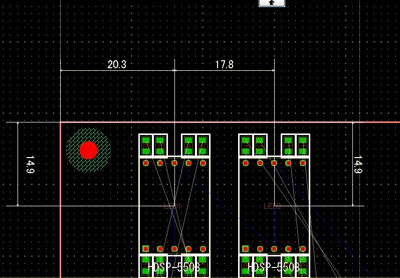
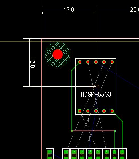
[LED1]、[LED2]の位置指定を行います。
[LED1]の位置を、基板左から17mm、基板上から15mm
[LED2]の位置を、[LED1]から左に25mm、基板上から15mmとします。
マウスの操作で、[LED1]を画面の中心位に全体移動します。
全体移動は、マウスの右ボタン押しながら移動させます。
さらに、マウスのホイールで画面を拡大します。
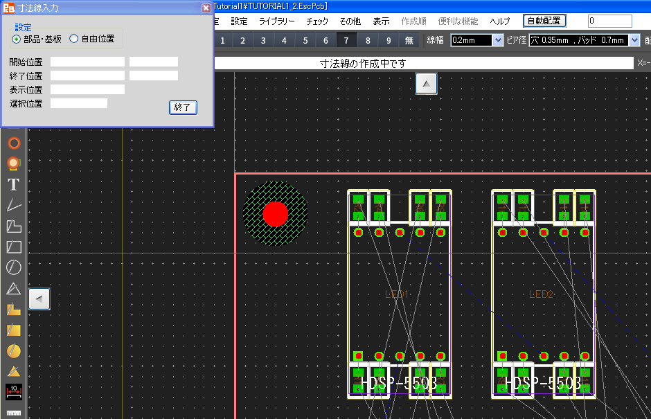
今回は寸法線による部品移動で部品を移動します。
メニュー[その他]->[寸法線の作成]を選択します。
すると寸法線作成の画面が表示されます。
The locations of [LED1] and [LED2] are going to be set as follows.
The location (coordinates) of [LED1] would be 17mm from the left edge of the board and 15mm from the top edge of the board.
The location (coordinates) of [LED2] would be 25mm from the location of [LED1] to left and 15mm from the top edge of the board.
Move the view of [LED1] to the center of the Drawing Area with a mouse operation.
Right-dragging can move the whole view in the Drawing Area.
Rotating a wheel of mouse can zoom up the view of the Drawing Area.
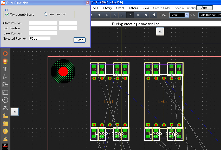
This time the component is going to be moved by changing a value of a dimension line as follows.
Select menu [Others]->[Create Dimension Line].
Then the following form for creating a dimension line appears.
4-3-1) [LED1]に寸法線を入れる
4-3-1) Draw Dimension Line at [LED1]
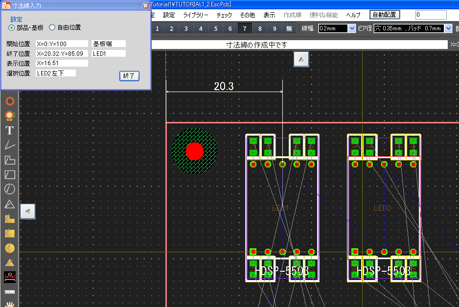
マウスを基板の左上端に移動し左クリックします。
次に、マウスを[LED1]の中心部分で左クリックします。
さらに、マウスを左右方向は基板の左上端と[LED1]の中間位の位置へ、上下方向は基板外形の上に移動し左クリックします。
これで[LED1]と基板左端からの左右方向の寸法が入りました。
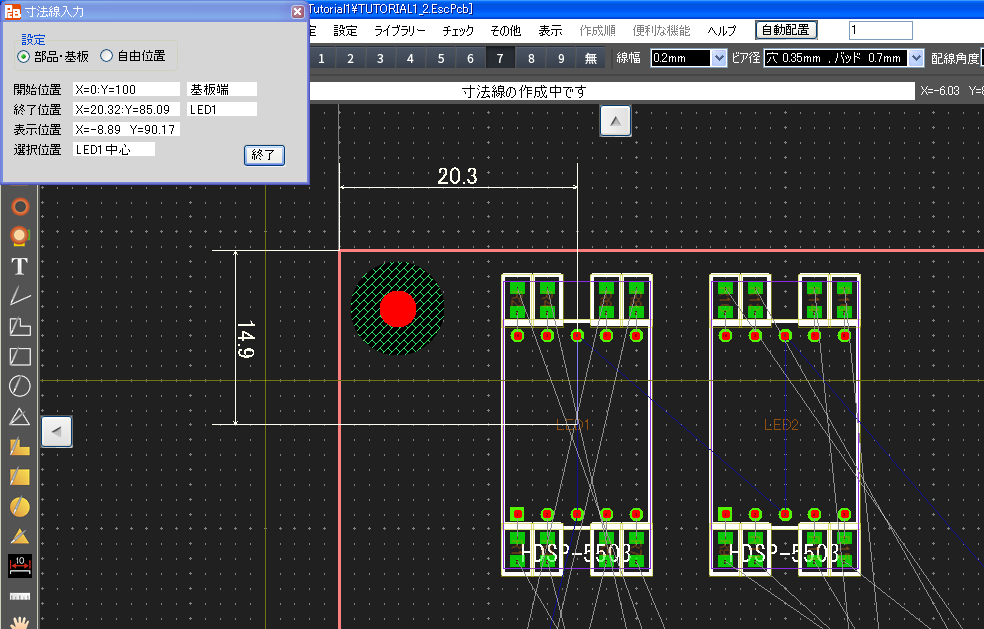
マウスを基板の左上端に移動し左クリックします。
次に、マウスを[LED1]の中心部分で左クリックします。
さらに、マウスを左右方向は基板の左上端よりも左へ、上下方向は基板の左上端と[LED1]の中間位の位置へ移動し左クリックします。
これで[LED1]と基板上端からの上下方向の寸法が入りました。
Move a cursor to the upper-left corner of the board and left-click there.
Next, left-click the center position of [LED1].
Continuously move a cursor around the center area between the left edge of the board and [LED1] for the horizontal direction and out of (upper side of) the board outline for the vertical direction then left-click.
Finally the horizontal dimension line between [LED1] and the left edge of the board has been created.
Move a cursor to the upper-left corner of the board and left-click there.
Next, left-click the center position of [LED1].
This time move a cursor out of the board outline (to left side of the left edge) for the horizontal direction and around the center area between the upper-left edge of the board and [LED1] for the vertical direction then left-click.
Finally the vertical dimension line between [LED1] and the upper edge of the board has been created.
4-3-2) [LED2]に寸法線を入れる
4-3-2) Draw Dimension Line at [LED2]
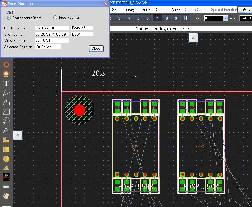
マウスを[LED1]の中心部分に移動し左クリックします。
次に、マウスを[LED2]の中心部分で左クリックします。
さらに、マウスを[LED1]と[LED2]の間、上下方向は基板外形の上に移動し左クリックします
これで[LED1]と[LED2]間の寸法が入りました。
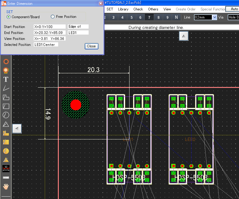
マウスを基板の左上端に移動し左クリックします。
次に、マウスを[LED2]の中心部分で左クリックします。
さらに、マウスを左右方向は[LED2]よりも右へ、上下方向は基板の左上端と[LED2]の中間位の位置へ移動し左クリックします。
これで[LED1]と基板上端からの寸法が入りました。
[LED1]、[LED2]共に寸法線が入りました。
[寸法線作成画面]の[終了]ボタンを押して、寸法線作成を終了します。
(ここまでのパターン図はTUTORIAL1_4.EscPcbになります)
Move a cursor to the center part of [LED1] then left-click.
Next, move a cursor to the center part of [LED2] then left-click.
Continuously move a cursor around the horizontal position between [LED1] and [LED2] and out of (upper side of) the board outline vertically then left-click.
Finally the (horizontal) dimension line between [LED1] and [LED2] has been created.
Move a cursor to the upper-left corner of the board and left-click there.
Next, move a cursor to the center part of [LED2] then left-click.
Continuously move a cursor to the right side of [LED2] horizontally and around the center area between the upper-left corner of the board and [LED2] vertically then left-click.
Finally the (vertical) dimension line between [LED1] and the upper edge of the board has been created.
Dimension lines of both [LED1] and [LED2] have been done.
Press the button [Close] in the form [Enter Dimension] then exit the creation of dimension line.

(The pattern data up to here is TUTORIAL1_4.EscPcb.)
4-4) 寸法線による部品移動
4-4) Move Component by Changing Dimension Value
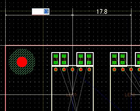
[LED1]と基板左端の距離が20.3mmなので、17mmに修正します。
“20.3”の数字の上にマウスを移動しダブルクリックします。
入力枠が出ますので、そこに"17エンター"と入力します。
当該部品が17mmの位置に移動しました。
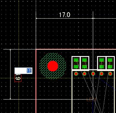
次に、基板上端から[LED1]までの距離を修正します。
14.9mmとなっていますので、15mmに修正します。
“14.9”の数字の上にマウスを移動しダブルクリックします。
入力枠が出ますので、そこに"15エンター"と入力します。
当該部品が15mmの位置に移動しました。

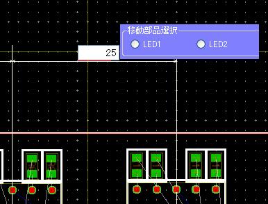
[LED1]と[LED2]の距離が21.1mmとなっていますので、25mmに修正します。
“21.1”の数字の上にマウスを移動しダブルクリックします。
入力枠が出ますので、そこに"25エンター"と入力します。
ここでは、[部品移動選択]画面が出ますので、[LED2]を左クリックします。
当該部品が25mmの位置に移動しました。
次に、基板上端から[LED2]までの距離を修正します。
14.9mmとなっていますので15mmに修正します。
“14.9”の数字の上にマウスを移動しダブルクリックします。
入力枠が出ますので、そこに"15エンター"と入力します。
当該部品が15mmの位置に移動しました。

(ここまでのパターン図はTUTORIAL1_5.EscPcbになります)
これで位置調整が終了しました。
The distance between [LED1] and the left edge of the board is going to be corrected from the present 20.3mm to 17mm as follows.
Move a cursor on the number "20.3" then left-double-click it.
Enter "17" in the entry field which has appeared then press the key [ENTER].
The component [LED1] has been moved to the position according to the distance "17mm".

Next, the distance between the top edge of the board and [LED1] is going to be changed as follows,
from the present value 14.9mm to the new 15mm.
Move a cursor on the number "14.9" and left-double-click it.
Enter "15" in the entry field which has appeared then press the key [ENTER].
That component [LED1] has been moved to the position of 15mm away.
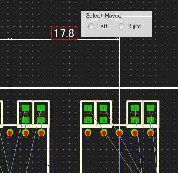
The distance between [LED1] and [LED2] is going to be changed from 21.1mm to 25mm as follows.
Move a cursor on the number "21.1" and left-double-click there.
Enter "25" in the entry field which has appeared then press the key [ENTER].
This time the small window [Select Moved] appears then left-click [LED2].
That component [LED2] has been moved to the position of 25mm away.
Next, the distance between the upper edge of the board and [LED2] is going to be corrected as follows
from 14.9mm to 15mm.
Move a cursor on the number "14.9" then left-double-click there.
Enter "15" in the entry field which has appeared then press the key [ENTER].
That component [LED2] has been moved to the position of 15mm away.
(The pattern data up to here is TUTORIAL1_5.EscPcb.)
Now the adjustment of the location has been done.
第5章 配線
Chapter 5. Wiring
5-1) 手動配線
5-1) Manual Wiring
[配線/ビア設定]エリアの[線幅]を"0.3mm"、[ビア径]を"穴 0.4mm バッド 0.8mm"、[配線角度]を"45度固定"に設定します

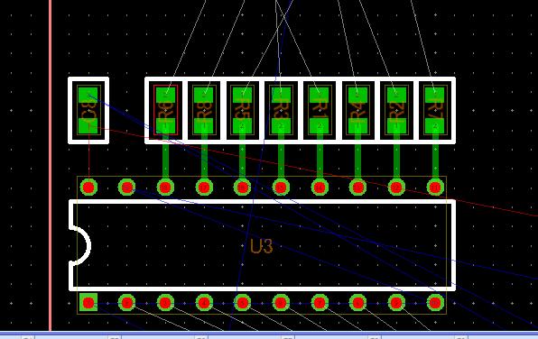
[U3]を、基板左端ぎりぎりまで移動します。
[R1]~[R8]までを、[U3]の近くに移動します。
(ここまでのパターン図はTUTORIAL1_6.EscPcbになります)
[R7-2]ピンを左クリックすると、[U3-11]まで白い点線が表示されます。
その線をなぞるように[U3-11]までマウスを移動させると、白い点線がグリーンの実線に変ります。グリーンはレイヤー1の色です。従って、レイヤー1にパターンを引いています。
[U3-11]の位置で左クリックすると、[R7-2]から[U3-11]までの配線が完了します。
このように、[R2-1]-[U3-12]、[R4-1]-[U3-13]、[R1-1]-[U3-14]、[R3-2]-[U3-15]、
[R5-2]-[U3-16]、[R8-1]-[U3-17]、[R6-1]-[U3-18]間を配線します。

(ここまでのパターン図はTUTORIAL1_7.EscPcbになります)
次に、[R1]~[R8]と[LED1]間までの配線をします。
グリッドは、パターンが[LED1]のピン間の真ん中を通るようにするため[2]にします。
[R7-1]上にマウスを移動し左クリックします。
[LED1-5]との間に白い点線がでます。
マウスを[LED1-5]まで移動し左クリックします

パターンが自動的に45度の角度を付け作成されました。
次に、[R2-2]~[LED1-10]までのパターンを引きます。
[R2-2]上にマウスを移動し左クリックします。
[LED1-10]まで移動させようとすると、線が赤くなり、[LED1-10]上でマウスを左クリックしても、配線は出来ません。
これは、他の線と電気的にショートしてしまう配線経路だからです。
[シフト]キーを押し45度の経路を変えても、線は赤のままで、パターンは引けません。
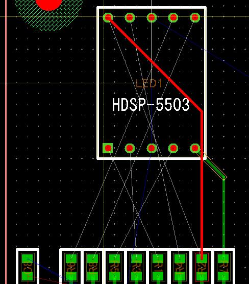
これは"リアルタイムDRC"機能により、配線時は常時ショートチェックを行っているからです。
●ここで"リアルタイムDRC"機能を説明します。
Set the [Line] "0.3mm", the [Via]"Hole 0.4mm, Pad 0.8mm" and the [W.Angle]"45 deg fixed" in the upper side of [the Drawing Area].

Move the component [U3] very close to the left edge of the board.
Move the eight components from [R1] to [R8] close to the component [U3].
(The pattern data up to here is TUTORIAL1_6.EscPcb.)
Left-click the pin [R7-2] then a white dotted line appears in between such pin and another pin [U3-11].
Move a cursor to the pin [U3-11] along such white dotted line then it changes to a green straight line. The green color means the one of layer-1, therefore the pattern has been drawn in layer-1.
Left-click the position [U3-11] then the wiring connection between [R7-2] and [U3-11] is completed.
By similar way do wiring between the following pads [R2-1]-[U3-12], [R4-1]-[U3-13], [R1-1]-[U3-14], [R3-2]-[U3-15],
[R5-2]-[U3-16], [R8-1]-[U3-17] and [R6-1]-[U3-18].
(The pattern data up to here is TUTORIAL1_7.EscPcb.)
Next, wiring between [R1]-[R8] and [LED1] is going to be done as follows.
Set the view grid to be [2] because in order for the pattern to go through the middle of two pins of [LED1].
Move a cursor on the pad [R7-1] and left-click there.
A white dotted line appears between there and the pad [LED1-5].
Move a cursor to the pad [LED1-5] and left-click there.
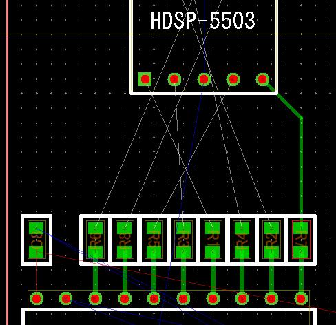
The pattern of which the angle is automatically 45 degrees has been drawn.
Next, a wired pattern between [R2-2] and [LED1-10] is going to be drawn as follows.
Move a cursor on the [R2-2] and left-click there.
Even though trying to move a cursor to the [LED1-10] and left-click there, the color of the line becomes red and its wiring cannot be done.
This reason is that this connection path would be electrically connected (short-circuited) to another pattern line.
Even if changing the path of 45 degrees with pressing the key [SHIFT], the line color remains red and wiring pattern cannot be done.

This reason is that short-circuit check is always doing during wiring by the function "Real-Time DRC"
The explanation of "Real-Time DRC" function is going to be mentioned as follows.
5-2) リアルタイムDRC
5-2) Real-Time DRC
配線中にマウスを移動させると、黄色円が一緒に移動します。
これは、マウスの現在地でビアを作成する事が可能であるというサインです。
ですから、他のパターンぎりぎりにマウスを移動させていくと、黄色円は消えてしまいます。
但し、黄色円が消えても、配線が赤色にならない限りは、パターンを引く事は可能です。
しかし、黄色円が消えてもなお、他のパターンぎりぎりにマウスを移動させていく、又は他のパターンと交差させると、今度は配線自体がショートしてしまう事を表す赤色になり、パターン作成は出来ません。
障害となる他のパターンは、黄土色でそのパターンを囲んでいます。
マウスを移動し、パターン作成に障害がなくなると、赤線は本来のレイヤー色に戻ります。
また、ビアを生成できる位置にマウスを移動すると、黄色円が再度表示されます。
パターン引きに戻ります。
現在、配線が赤色になっている為、パターンを迂回させて引かなくてはなりません
[R2-2]と[LED1-5]中間点までマウスを真上に移動させます
その場所でマウスの真ん中のボタンを押すと、ビアが発生します。
白い点線はビアの場所から[LED1-10]の間になります。
ここで真ん中のボタンを離しマウスを左に移動させると、パターンの色がグリーンから茶色に変ります。これはビアが発生したので、自動的に配線レイヤーが変った為です。
マウスを左に移動させ、[LED1-10]よりも少し左側で真ん中のボタンを押します。
次に、マウスを[LED1-10]まで移動させ左クリックします。

このようにして[R6-2]までのパターンを引きます。
(ここまでのパターン図はTUTORIAL1_8.EscPcbになります)
図を見て分るように、パターンを引くと細い白い線(ラッツネット)は消えます。
Moving a cursor during wiring moves a yellow circle together normally.
This is the indication that a via can be created at the present cursor's position.
Therefore if a cursor is located very close to the other pattern, a yellow circle disappears.
But even if a yellow circle disappears, a pattern can be drawn unless the color of the wiring line becomes red.
But moving a cursor more close to the other pattern even a yellow circle disappears or crossing a wiring line with the other pattern makes its color to be red which indicates short-circuit and impossibility of pattern creation.
Such other obstructive pattern becomes surrounded with the ocher color.
Moving a cursor away from such obstruction makes the line color (red) return to the original layer's color.
Also, moving a cursor away to the position where a via can be created makes the yellow circle appear again.
Let's get back to the subject to wiring pattern issue.
Because the color of the wiring line is red at present, the pattern should be wired with diverting the obstruction.
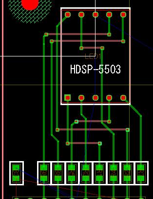
Move a cursor to the middle position between [R2-2] and [LED1-5].
Press and hold the wheel button of mouse at that position then a via is generated.
The white dotted line gets to appear between the via's position and [LED1-10].
Now release the wheel button and move a cursor to left then the color of pattern line changes from green to brown. This is because the wiring layer has been changed automatically due to via's generation.
Move a cursor to left and press the wheel button at the position a bit left to [LED1-10].
Next, move a cursor to the pad [LED1-10] then left-click there.
By similar way do wiring patterns of [R3-2][R4-2][R5-2][R6-2].

(The pattern data up to here is TUTORIAL1_8.EscPcb.)
After the pattern has been drawn, the thin white line (Ratsnet) disappears as the above figure shows.
5-3) 配線中の[シフト]キーと[スペース]キー
5-3) Functions of Keys [SHIFT] and [SPACE] during Wiring
配線中の[シフト]キーの動きは、部品移動中とは異なります。
配線中に[シフト]キーを押すと、配線45度の角度が逆さになります。
もう一度[シフト]キーを押すと元に戻ります。
この繰り返しを行います。
[スペース]キーは、配線レイヤーを変えます。
1度押すと、配線レイヤーは最後のレイヤーに近いレイヤー(現在の場合はレイヤー4)になり、再度押すと元に戻ります。
初期での配線レイヤーは、レイヤー1と最後のレイヤーです。
レイヤー指定を変えると、[スペース]キーで変える事の出来るレイヤーが変ります。
(詳細は取り説を参照して下さい)
The function of pressing the key [SHIFT] during wiring is different from the one during moving component.
Pressing the key [SHIFT] during wiring makes the wiring angle of 45 degrees inverted.
Pressing the key [SHIFT] again returns it to be original.
In brief pressing the key [SHIFT] toggles the angle of 45 degrees between the abovementioned two states.
Pressing the key [SPACE] changes the wiring layer.
Pressing it once changes the layer to the bottom one (Layer-4 in this case initially) and pressing it again returns it to the original one.
The two layers which can be switched by pressing [SPACE] are initially the top and bottom ones.
Changing one of such two layers to another layer by right-clicked menu's command during wiring swaps it for the new (such another) layer.
(Refer to the operation manual for more detail.)
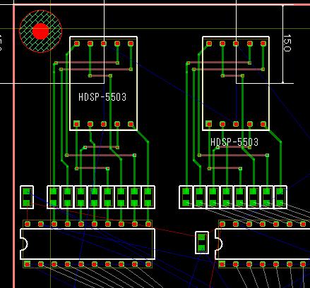
5-4) [LED2]のパターンを引く
5-4) Draw Pattern of [LED2]
[同一部品レイアウト]機能によりパターンを引きます。
[LED1]上にマウスを移動し、右クリックするとメニューが表示されます
[同一部品レイアウト]の場所にマウスを移動すると、右にサブメニューが出ますので、
その中から[LED2]を選択します。
すると、[LED1]と同じ部品グループ内の配線が、瞬時に出来上がります。

グリッドを[7](1.27mm)にし、後は[U4]を左に移動させて、[R8]-[R16]までと[U4]の間の結線をするだけです
(ここまでのパターン図はTUTORIAL1_9.EscPcbになります)
以上の5-1)、5-2)を繰り返し、パターンを引いていきます。
Wiring pattern is going to be done with the function [Same Component Layout] as follows.
Move a cursor on the [LED1] and right-click in order to open a popup menu.
Select (move a cursor on) [Same Component Layout] then a sub menu appears to right.
Select [LED2] in that list.
Then the layout (wiring) pattern of [LED2] component group is completed immediately and same as the one of [LED1] component group.
Set the view grid [7](1.27mm) and finally move [U4] to left and just wire between [R8]-[R16] and [U4].
(The pattern data up to here is TUTORIAL1_9.EscPcb.)
Continue to draw patterns with repeating the way of the abovementioned chapter 5-1) and 5-2).
5-5) パターンを引きなおしたい時、削除、修正
5-5) Re-Draw, Delete or Change Pattern
パターンを引いている途中で、パターンを引きなおしたい時は、[CTRL]+[Z] を押します。すると1つ手前に戻ります。
一旦パターンを引き終わってからの場合は、削除、修正になります。
削除は、マウスを削除したいパターン上に置くと、赤枠で囲まれた選択状態となりますので、[DEL]キーを押すと、そのパターンが削除さます。また[CTRL]+[Z]で1つ手前まで戻す事が出来ます([UNDO]機能)。
移動は、マウスを移動したいパターン上に置くと、赤枠で囲まれた選択状態となりますので、マウスの左ボタンを押しながら移動すると、そのパターンが移動します。
パターンの引きなおし
マウスを引きなおしたいパターン上に置きます。左クリックし、パターンを引き始めます。
引き始めた線上でパターン引きを終了すると、旧パターンは自動的に消え、引きなおしになります。
結線が終わった表示が下記になります。
(ここまでのパターン図はTUTORIAL1_10.EscPcbになります)
If pattern should be re-drawn during pattern drawing, press the keys [CTRL]+[Z] to back to the previous state.
If it should be done after pattern completed, use deletion or change.
In case of deletion move a cursor on the pattern which should be deleted then it becomes selected with a red frame surrounded then press the key [DEL] to delete such pattern. Also pressing the keys [CTRL]+[Z] can back to just previous state ([UNDO] function).
In case of movement move a cursor on the pattern which should be moved then it becomes selected with a red frame surrounded then left-drag to move such pattern.
Re-drawing pattern:
Put a cursor on the pattern which should be re-drawn. Left-click there to start drawing a pattern.
In order to cancel drawing after start drawing, press the key [ESC] or select "Cancel" in the popup menu opened by right-click. The previous pattern disappears automatically and it becomes ready to re-draw.
The result of the view after wiring completed is as follows.

(The pattern data up to here is TUTORIAL1_10.EscPcb.)
第6章 ベタパターンの生成
Chapter 6. Create Solid Filling Pattern (Plane Pattern)
6-1) 面積が小さいベタパターンの作成
6-1) Create Small Area of Solid Filling Pattern
この回路図では、
①電源入力の+12Vのラインは、ネット名[+12V]
②[U2]の電源は[L1]で分離されていますので、ネット名[N75374]
2種類のベタパターンを作成します。
In this circuit
Two solid filling patterns as follows are going to be created.
(1) The net name [+12V] of which line is a power supply +12V
(2) The net name [N75374] which line is a power supply [U2] separated by [L1]
6-1-1) +12Vラインのベタパターンの作成
6-1-1) Create Solid Filling Pattern of "+12V" Line
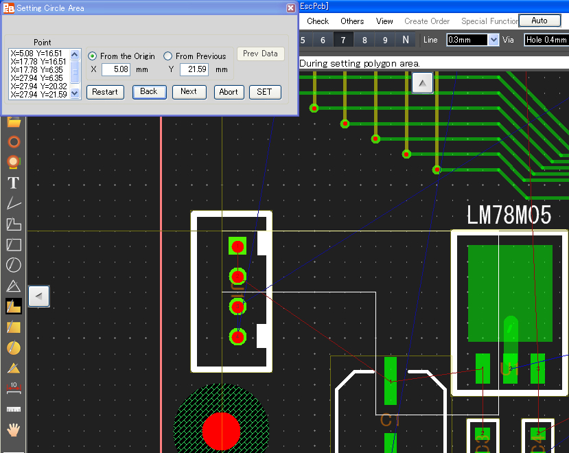
メニュー[設定]->[ベタパターン生成]を選択します。
[図形選択]画面が出ますので、[多角形]を選択します。
[ポリゴンエリア設定]画面が表示されます。
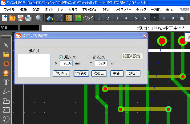
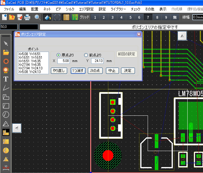
まず、多角形のエリアを指定します。
指定方法は、マウスで多角形の始点の位置を左クリック、次の頂点までマウスを移動し左クリック、更に次の頂点まで移動し左クリックしていきます(頂点と頂点を結ぶ白い線が引かれます)。
多角形のエリアの指定を終了したい時は、始点と終点を重ねます。
すると、[ベタ面設定]画面に自動的に移行します
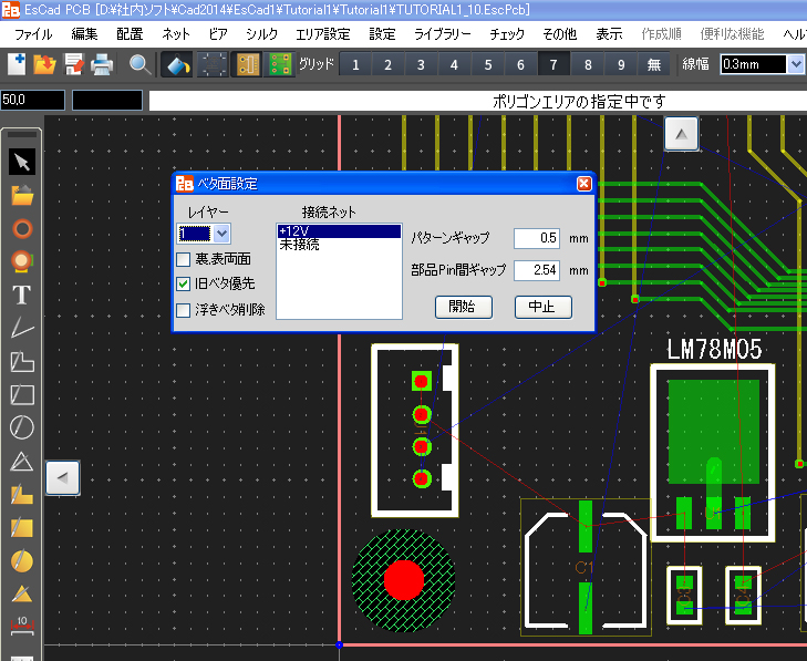
[レイヤー]を1に設定(そのまま)します。
[接続ネット]を"+12V"(そのまま)にします。
[開始]ボタンを押します。
数秒後ベタパターンが完成します。
Select menu [SET]->[Create Solid Filling Pattern].
The small form [Select Figure] appears and select [Polygon].
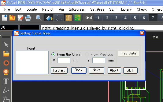
The window [Setting Polygon Area] is opened.
First, specify the area of polygon.
Its method is that left-click the position which is the first corner of the polygon, move a cursor to the next corner then left-click there and move again a cursor to the next corner then left-click there. Continue to do this sequence. (A white line continues to appear in between two corners.)
At last for finishing specifying the polygon area move a cursor to the first corner then left-click there.
Then the form [Set Solid Filling Pattern] appears.
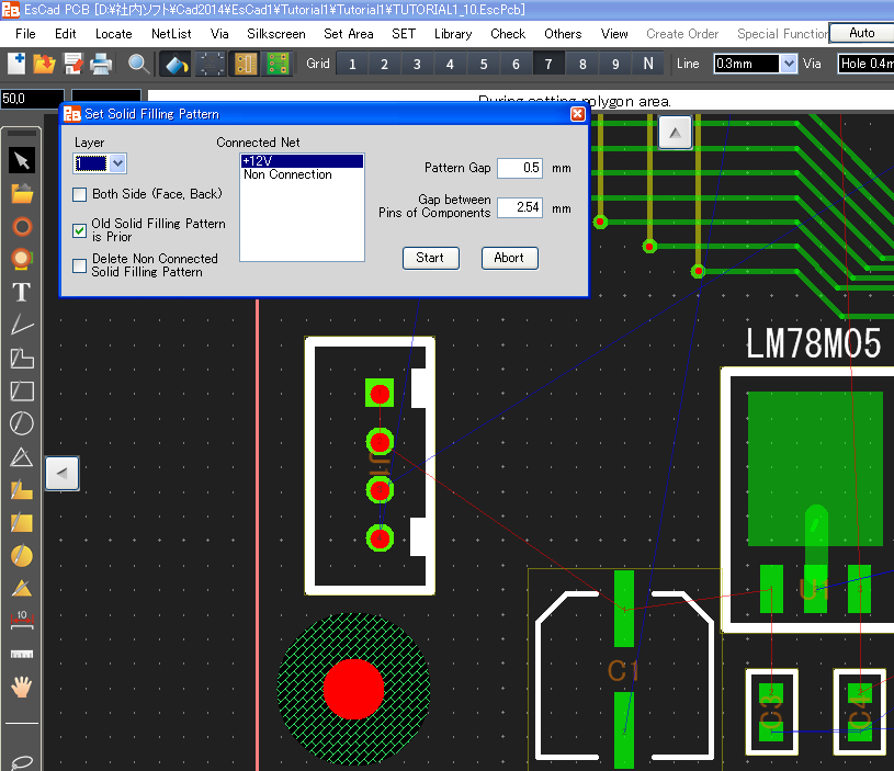
Set [Layer] to be 1 (as it is).
Set [Connected Net] to be "+12V" (as it is).
Press the button [Start].
After several seconds, the solid filling pattern is completed.

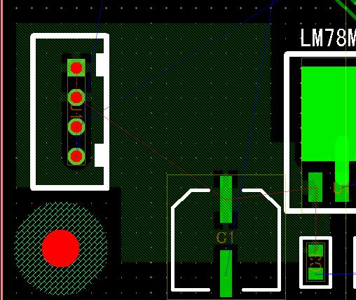
6-2) ネット名[N75374]のベタパターン作成
6-2) Create Solid Filling Pattern of the net name [N75374]
レイヤー3にベタパターンを作成しますので、事前に接続ビアを作成します
[U2-24]と[C9-2]にパターンを作成し、中間点の位置にビアを作成します。
[U2-32]と[C7-1]にパターンを作成し、中間点の位置にビアを作成します。
[U2-48]と[C6-2]にパターンを作成し、中間点の位置にビアを作成します。
[U2-71]と[C5-1]にパターンを作成し、中間点の位置にビアを作成します([C5]は半田面実装ですので注意が必要です)。
[L1-2]からパターンを引き、途中でビアを作成します。
ビアの作成が終わったら、[ESC]キーで配線モードを解除します。
下図左上の位置にマウスを移動し(x=50.8mm,y=38.0mm付近)マウスの左ボタンを押します。
左ボタンを離さずX=72.4mm、Y=14.0mm付近までマウスを移動させ領域指定をします。
マウスの移動位置は、画面上に X=50.81 Y=38.05のようにリアルタイムで表示しています。
マウスの左ボタンを離し、その位置でマウスを右クリックすると、メニューが表示されます。
[ベタパターン]を選択します。
[レイヤー]を3に設定します。
[接続ネット]を"N75374"(そのまま)で、[開始]ボタンを押します。
数秒後ベタパターンが完成します。

(ここまでのパターン図はTUTORIAL1_11.EscPcbになります)
A connected via is going to be create in advance as follows because a solid filling pattern is going to be created in Layer-3.
Create a wired pattern between [U2-24] and [C9-2] then create a via at its midpoint.
Create a wired pattern between [U2-32] and [C7-1] then create a via at its midpoint.
Create a wired pattern between [U2-48] and [C6-2] then create a via at its midpoint.
Create a wired pattern between [U2-71] and [C5-1] then create a via at its midpoint. (Be careful of the component [C5] which is located in the solder side.)
Draw a pattern from [L1-2] then create a via on its way.
After vias created, press the key [ESC] to release the wiring mode.

Move a cursor to the upper-left position as the following figure mentioned (its coordinates are around X:50.8mm and Y:38.0mm) then left-click and hold there.

Continuously left-drag to the position of which coordinates are around X:72.4mm and Y:14.0mm for specifying the area.
A cursor's position (coordinates) is shown at the top of the display such as X=50.81 Y=38.05 in real time.
Release the left button and right-click its position then a form appears.
Select [Solid Filling Pattern].
Set [Layer] to be 3.
Leave [Connected Net] to be "N75374" (as is it) then press the button [Start].
After several seconds, the solid filling pattern is completed.
(The pattern data up to here is TUTORIAL1_11.EscPcb.)
6-3) 大きなベタパターンの作成
6-3) Create Large Solid Filling Pattern
6-3-1) レイヤー2に"GND"ベタパターン作成
6-3-1) Create Solid Filling Pattern of "GND" in Layer 2
マウスホイールで画面の拡大・縮小、マウス右ボタンを押しながら基板位置を移動し、基板の全体が見えるように位置を合わせます
基板の左上(パターン、部品、ビアの無い位置)でマウスの左ボタンを押し、左ボタンを押しながらマウスを基板の右下まで移動します。
マウスの左ボタンを離し、マウスの右ボタンでメニューが表示されます。
[ベタパターン]を選択します。
[ベタ面設定]画面が開きます。
レイヤー設定]を”2”に設定します
[接続ネット]は"GND"を選択し、[開始] ボタンを押します。
数秒後ベタパターンが完成します。
Fit the whole view of the board in the Drawing Area by zooming up & down with a mouse's wheel or moving the position with right-dragging.
Left-click and hold the upper-left position of the board (where there is no patters, components or vias) then left-drag to the lower-right of the board.
Release the left button and right-click for opening a popup menu.
Select [Solid Filling Pattern].
A form [Set Solid Filling Pattern] appears.
Set [Layer] to be "2".
Select "GND" in [Connected Net] then press the button [Start].
After several seconds, the solid filling pattern is completed.
6-3-2) レイヤー3に"+5V"ベタパターンの作成
6-3-2) Create Solid Filling Pattern of "+5V" in Layer 3
基板の左上(パターン、部品、ビアの無い位置)でマウスの左ボタンを押し、左ボタンを押しながらマウスを基板の右下まで移動します
マウスの左ボタンを離し、マウスの右ボタンでメニューが表示されます。
[ベタパターン]を選択します。
[ベタ面設定]画面が開きます。
[レイヤー設定]を”3”に設定します。
[接続ネット]は"+5V"を選択し、[開始] ボタンを押します。
数秒後ベタパターンが完成します。
Left-click and hold the upper-left position of the board (where there is no patters, components or vias) then left-drag to the lower-right of the board.
Release the left button and right-click for opening a popup menu.
Select [Solid Filling Pattern].
A form [Set Solid Filling Pattern] appears.
Set [Layer] to be "3".
Select "+5V" in [Connected Net] then press the button [Start].
After several seconds, the solid filling pattern is completed.
6-3-3) レイヤー1,4に"GND"ベタパターンの作成
6-3-3) Create Solid Filling Pattern of "GND" in Layer 1 and 4
基板の左上(パターン、部品、ビアの無い位置)でマウスの左ボタンを押し、左ボタンを押しながらマウスを基板の右下まで移動します
マウスの左ボタンを離し、マウスの右ボタンでメニューが表示されます。
[ベタパターン]を選択します。
[ベタ面設定]画面が開きます。
[裏,表両面]にチェックをいれます。
[接続ネット]は"GND"を選択し、[開始] ボタンを押します。
多少の時間がかかりますが、ベタパターンが完成します。
(ここまでのパターン図はTUTORIAL1_12.EscPcbになります)
Left-click and hold the upper-left position of the board (where there is no patters, components or vias) then left-drag to the lower-right of the board.
Release the left button and right-click for opening a popup menu.
Select [Solid Filling Pattern].
A form [Set Solid Filling Pattern] appears.
Set [Both Side (Face, Back)] checked on.
Select "GND" in [Connected Net] then press the button [Start]
After a while, the solid filling pattern is completed.

(The pattern data up to here is TUTORIAL1_12.EscPcb.)
第7章 未接続ピンの確認
Chapter 7. Check Non-Connected Pins
メニュー[チェック]->[未接続]を選びます。
画面の右側に[未接続ピン]画面が表示され、未接続ピン一覧が表示されます。
基板図の中の未接続ピンが白色点滅します
未接続ピン一覧の[C10-1]を左クリックすると、[C10-1]が赤点滅に変り、画面の中央に移動します。
[C10-1]を接続しましょう。
[未接続ピン]画面を閉じます。
ここでは、[C10]の配置が上下逆さになっているようですので、マウスを[C10]の上に置き、右クリックでメニューを開き、[回転]->[反転]を選択します。すると下図のようになりますので、"はい"を選択します。
数秒後、[C10]の上下が正常に戻り、かつベタパターンが作り直されます。
次に、[C10-1]と[U4-20]をパターン接続します。
すると、またメッセージが出ますので、"はい"を選択します。
数秒後、ベタパターンが作り直さます。
次に、[C12-1]から右にパターンを引き、[U5-20]の位置でビアを打ちます。
その後、[ESC]キーでパターン描画モードを抜けます。
ベタパターンは自動修正されます。

このように、未接続ピンを結線していきます。ベタパターンは自動修正されます。
[U2-70]は、グリッドを[2]にしてパターンを通します。
(ここまでのパターン図はTUTORIAL1_13.EscPcbになります)
未接続を全て接続すると、ラッツネットの線は全て消えます。
Select menu [Check]->[Non Connection].
A form of [Non Connected Pin] appears in the right side of display and shows the list of non connected pins.
The view of non connected pin in the Drawing Area flashes with a white color.
Left click [C10-1] in such list then the view of [C10-1] in the Drawing Area changes to flashing with a red color and its position becomes in the center of Drawing Area.
Let's connect [C10-1].
Close the form [Non Connected Pins].
Here the placement of [C10] is upside-down. Move a cursor on [C10], right-click there for opening a popup menu and select [Rotate]->[Flip]. Then the view becomes like the following figure and select "Yes".
After several seconds, the direction of [C10] becomes correct and the solid filling pattern is re-created as well.
Next, draw a pattern connected between [C10-1] and [U4-20].
Then the message appears again and select "Yes".
After several seconds, the solid filling pattern is re-created.

Next, draw a pattern from [C12-1] to right and create a via at the position of [U5-20].
After that, press the key [ESC] for releasing the drawing pattern mode.
The solid filling pattern is corrected automatically.
Thus, continue to wire non connected pins. The solid filling pattern is corrected automatically.
Pass the pattern for [U2-70] to set the view grid [2].

(The pattern data up to here is TUTORIAL1_13.EscPcb.)
After all of the non connected pins are connected, all the ratsnet lines disappear.
第8章 ユニバーサルエリアの作成
Chapter 8. Create Universal Pattern Area
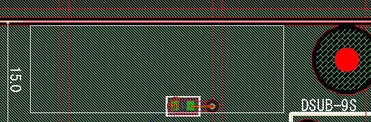
ここでは、基板の右上に空いているエリアが有りますので、ここにユニバーサルエリアを作成します。
下図のようにエリア選択をします
ここでのエリアは四角形になりますので、2本ある対角線のいずれか一方の始点(必ずパターン、部品、ビアの無い位置)で、マウスの左ボタンを押したまま終点まで移動し、左ボタンを離します。
注)このエリアの中には、必ず最低1つの、パターン、部品、ビアのいずれかを入れて下さい。入っていないと、エリア選択はされません。
エリア選択をしたら、マウス右クリックでメニューを表示します。
メニューの中から、[ユニバーサルエリア発生]を選択します。
すると、下図のように[ユニバーサルエリア発生]画面が表示されますので、
[穴径]を"0.8"、[パッド径]を"1.2"にそれぞれ設定し、[開始]ボタンを押します。
ユニバーサルエリアは、ベタパターンの再作成を行わない場合はすぐに作成されますが、ベタパターンの再作成を行う場合は、多少の時間がかがります
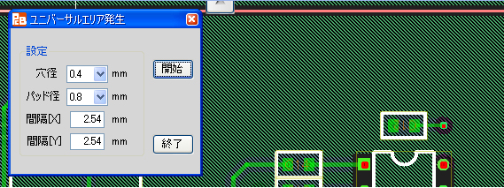
終了すると、[ユニバーサルエリア発生]画面が消えます。
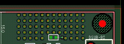
(ここまでのパターン図はTUTORIAL1_14.EscPcbになります)
A universal pattern area is going to be created in the empty space in the upper-right part of the board as follows.
Do area selection as the following figure.
A rectangle has selected here so that left-drag a corner of rectangle, move then release it at its diagonal position in the area of no patterns, components or vias.
Note) After the area has been created, any one of patterns, components or vias should be created at least in such area. If nothing in such area, its area selection cannot be done.

After the area selection, right-click in such area to open a popup menu.
Select [Generate Universal Area] in the menu.
Then the following form of [Generate Universal Area] appears.
Enter "0.8" in [Hole Diameter] and "1.2" in [Pad Diameter] then press the button [Start].
This universal area is created immediately in case of no re-creating solid filling pattern but it takes a while in case of doing re-creation.
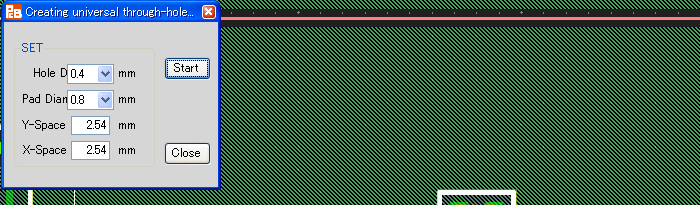
After its completion, the form of [Generate Universal Area] is closed.

(The pattern data up to here is TUTORIAL1_14.EscPcb.)
第9章 GND補強ビアの取り付け
Chapter 9. Create Vias for Strengthening GND Impedance
まず、基板全体をエリア選択します。
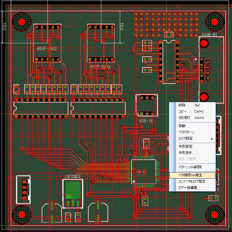
エリア選択したら、マウス右クリックでメニューを表示します。
メニューの中から、[ベタ接続ビア発生]を選択します。
すると、下図のように[自動穴作成]画面が表示されますので、[穴径]を"0.6"にします。
[接続ネット]エリアの中から"GND"を選択し、[開始]ボタンを押します。
GND補強ビアが発生し、[自動穴作成]画面が消えます。
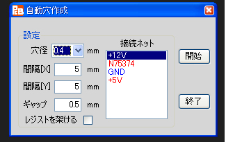
ここでは、ベタパターンの再生性が4層分になるので、多少の時間がかがります
(ここまでのパターン図はTUTORIAL1_15.EscPcbになります)
First, do area selection of the whole of the board.
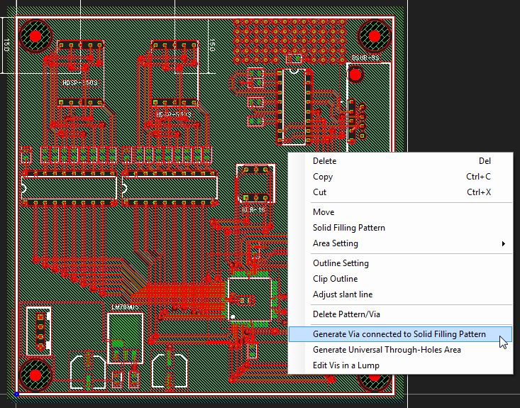
After that, right-click to open a popup menu.
Select [Generate Via Connected to Solid Filling Pattern] in the menu.
Then the following form of [Auto Hole Creation] appears and enter "0.6" in the field of [Hole Diameter].
Select "GND" in the area of [Connected Net] then press the button [Start].
The vias for strengthening GND impedance are created and the form of [Auto Hole Creation] is closed.
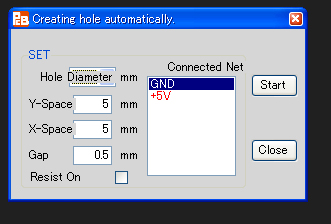
In this case it takes a while to be completed because re-creation of solid filling pattern is done for four layers.
(The pattern data up to here is TUTORIAL1_15.EscPcb.)
第10章 シルク生成
Chapter 10. Create Silkscreen
10-1) リファレンスシルクの生成
10-1) Create Silkscreen of Reference Name
メニュー[シルク]->[全部品リファレンスシルク生成]を選択します。
すると、全ての部品のリファレンスのシルク(シルク文字)が生成されます。
このシルクを、部品によっては適切な位置に移動させます。
シルクの移動は、移動させたい文字の上にマウスを置くと、当該文字が赤枠で囲まれますので、マウスの左ボタンを押したまま移動させ、左ボタンを離します。

Select menu [Silkscreen]->[Generate Reference Silkscreen of All Components].
Then silkscreens (text) of the reference names of all components are generated.
Move those silkscreens to the intended positions if necessary.
The way of moving silkscreen is that, put a cursor on the text to be moved then the text is surrounded with a red frame and left-drag it then release the mouse button at the intended position.
10-2) 部品名シルクの生成
10-2) Create Silkscreen of Component Name
ICなどでは、部品名を入れた方が良い場合があります。
部品名の上にマウスを移動し、右クリックでメニューを表示します。
メニューの中から、[部品名シルク生成]を選択すると、部品名のシルクが生成されますので、適切な位置に移動させて下さい。
In case of a component such as IC, it is better to draw a silkscreen of the component name.
Put a cursor on the component name then right-click for opening the popup-menu.
Select [Create Silkscreen of Component Name] in the menu then a silkscreen of the component name is generated and move it to the intended location.

10-3) その他シルクの生成
10-3) Create Another Silkscreen
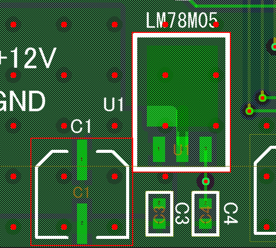
電源コネクターの近くに、入力電圧を入れてみましょう。
メニュー[シルク]->[文字]を選択します。
すると、[文字編集]画面が現れます。
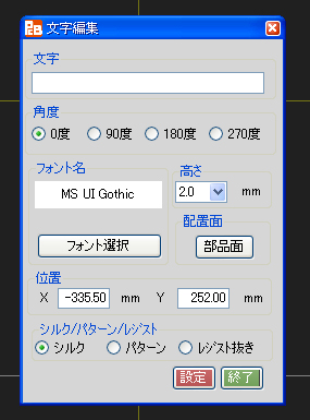
[文字]の入力欄に、"+12V"と入力します(入力文字は自由で、漢字の入力も可能です)。
文字の高さを"3.0"mmにします。
文字を置きたい位置にマウスを移動し、左クリックで確定します。
続けて、他のシルク文字を入れたい場合は、上記の操作を繰り返します。
また、パターン、レジスト抜きでも入力する事ができます。
(ここまでのパターン図はTUTORIAL1_16.EscPcbになります)
Let's create a silkscreen of the input voltage value near a power connector.
Select menu [Silkscreen]->[Character].
Then the form of [Edit Character] appears.
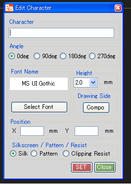
Enter "+12V" in the field of [Character].
Set the character height to be "3.0"mm.
Move the character with mouse operation then left-click the position to be put for settlement.
Repeat the above procedures if continuing to create another silkscreen character.
This creation can be done by not only silkscreen but also pattern or clipping resist.
(The pattern data up to here is TUTORIAL1_16.EscPcb.)
第11章 ロゴ(イラスト)の入力
Chapter 11. Draw Logo (Illustration)
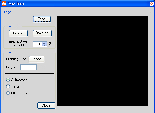
メニュー[シルク]->[ロゴ挿入]を選択します。
すると、[ロゴ挿入]画面が現れます。
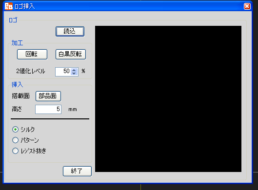
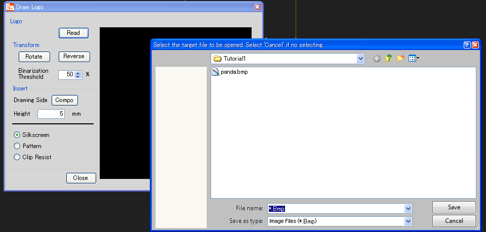
[読込]ボタンを押します。
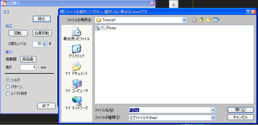
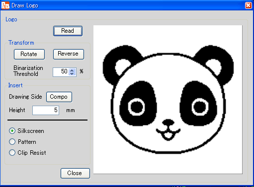
今回はイラストの”パンダ.bmp”を選択します。
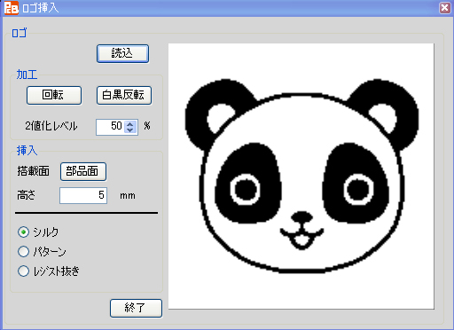
高さを”10mm”にします。
マウスを移動すると、赤色のロゴイメージが一緒に移動します。
ロゴを置きたい場所で、左クリックします。
すると、[ロゴ挿入]画面が消え、下記のようにロゴが入ります。
また、パターン、レジスト抜きでも入力する事ができます。

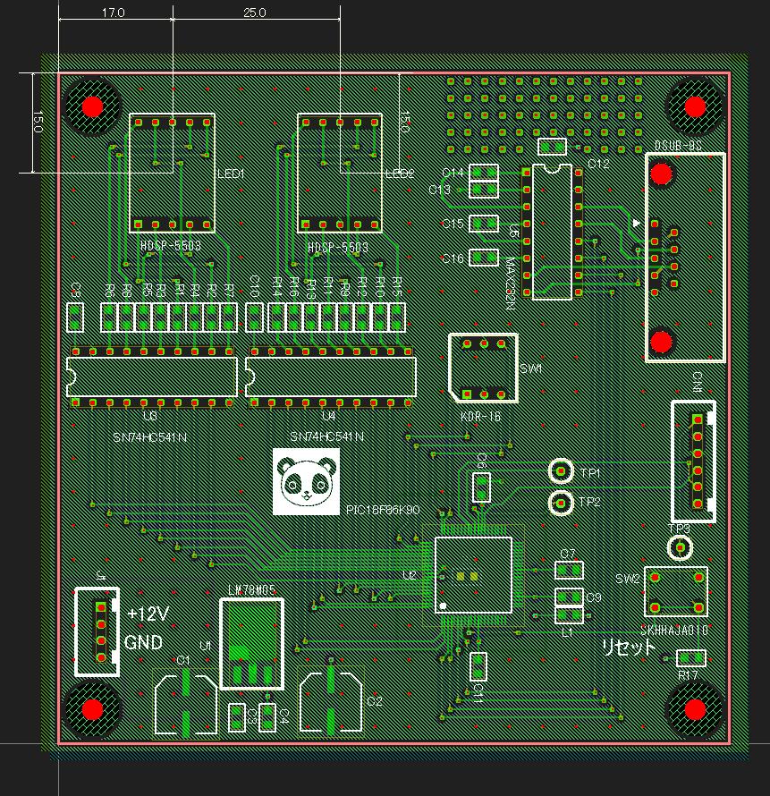
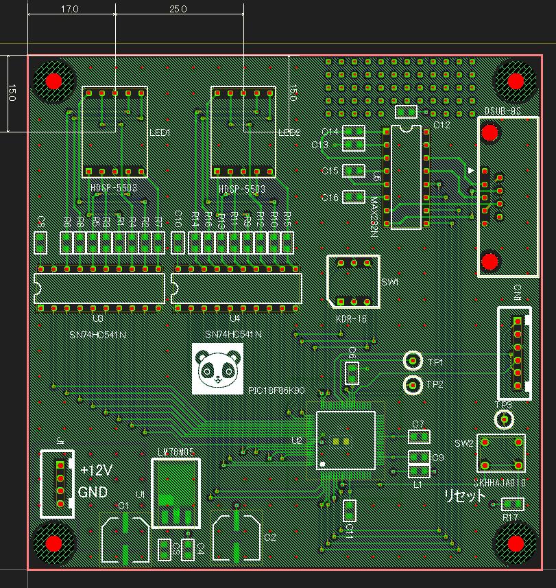
(ここまでのパターン図はTUTORIAL1_17.EscPcbになります)
Select menu [Silkscreen]->[Draw Logo].
Then the form [Draw Logo] appears.
Press the button [Read].
Select "panda.bmp" file of an illustration for this time.
Set the height "10mm".
Move the mouse then the red logo image is also moved together.
Left-click the position where the logo should be placed.
Then the form [Draw Logo] is closed and the logo is drawn as follows.
It can be drawn by using pattern or clipped resist as well.
(The pattern data up to here is TUTORIAL1_17.EscPcb.)
第12章 仕上げ
Chapter 12. Finishing Touches
12-1) 未接続ベタの削除
12-1) Delete Floating Solid Filling Pattern
メニュー[設定]->[未接続ベタ削除]を選択します。
すると、下図のようになります。
Select menu [SET]->[Delete Non Connected Solid Filling Pattern].
Then the view becomes as follows.

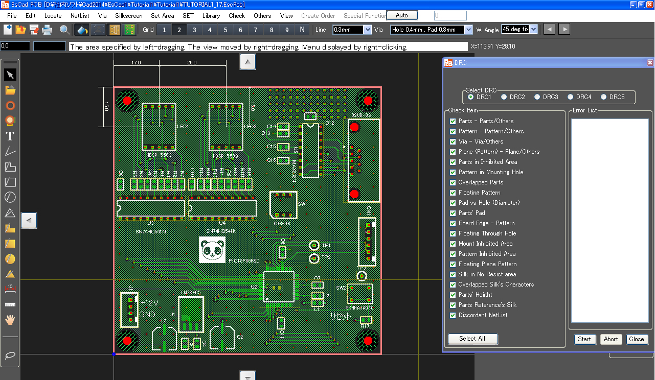
12-2) DRC(デザインルールチェック)
12-2) DRC (Design Rule Check)
メニュー[チェック]->[DRC]を選択します。
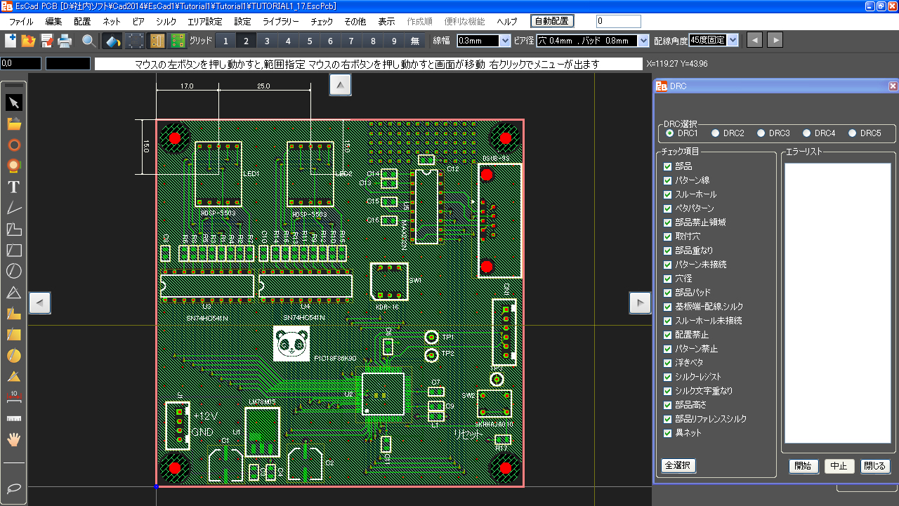
[DRC]画面が出ます。
[開始] ボタンを押します。
DRC終了までには、多少の時間がかかります。
終了すると、[エラーリスト]内にここまでのエラーを表示します。
[エラーリスト]内のエラー項目をマウスで左クリックすると、その項目に該当するエラー箇所が、画面上赤枠で囲まれて拡大表示されます(異ネットエラーは表示されません)。
下図は、ここでのエラーリストに表示された、最初のエラー項目に該当するエラー箇所です。

エラーは、[DRC]画面が開いたままでも修正可能です。
上図は、パターン修正を行った様子です。
各々の修正が終了したら、一旦[DRC]画面を閉じ、メニュー[設定]->[未接続ベタ削除]を再度実行します。
これは、パターンやビア位置等の修正によるベタパターンの再生性が行われた際に、未接続ベタパターンが発生しているからです。
[DRC] -> 修正 を繰り返して、DRCのエラーを減らしていきます。
今回の場合、最後まで、以下のようなエラーが1つの残りました、
“CN2シルクが外形に隣接又は外”というエラーです。
このエラーの修正は、今回は行いません。
このように、[DRC]でエラーとなった場合でも、基板製造に特段の問題が無い、と判断した場合には、修正しなくても支障ありません。

(ここまでのパターン図はTUTORIAL1_18.EscPcbになります)
Select menu [Check]->[DRC].
The [DRC] window appears.
Press the button [Start].
It takes a while for DRC to finish.
After finish, errors are listed in the [Error List].
Left-click the listed item in the [Error List] then the view of Drawing Area is changed to show its concerned position zoomed in and surrounded with a red frame (no change in case of error of "Discordant NetList").
The following figure shows the position corresponded to the first item listed in the Error List.
An error part can be fixed during the window [DRC] opened.

The above figure shows the revision of patterns done.
After each revision completed, close the window [DRC] once and execute menu [SET]->[Delete Non Connected Solid Filling Pattern] again.
It is because some floating solid filling pattern may be created after re-generating solid filling pattern due to correcting patterns or vias' location.
Repeat executing [DRC] and correcting for decreasing the errors of DRC.
In this case one error remains as follows finally.
It is "Over b.outline Figure by Silkscreen by No.19".
Now it is not corrected.
Thus it is no problem not to correct in case of being able to judge there is no trouble for producting the actual board even if there is an error of [DRC].
(The pattern data up to here is TUTORIAL1_18.EscPcb.)
第13章 印刷
Chapter 13. Print Out
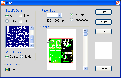
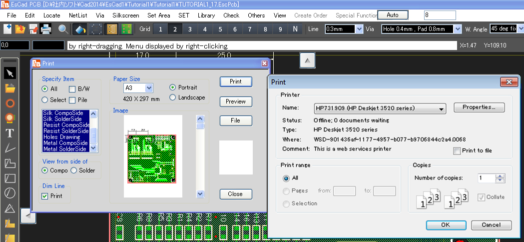
基板図を印刷します。
メニュー[ファイル]->[印刷]を選択します。
下図のように、[印刷]画面が表示されます。
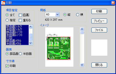
印刷は、自動スケールになっていますので、用紙から基板図がはみ出ることは有りません
今回は、[項目指定]枠の[白黒]にチェックを入れます。
[寸法線]枠の[印刷]にチェックを入れます。
用紙を設定して、[印刷]ボタンを押します。
すると、印刷選択画面が現れますので、それにしたがって印刷をします。
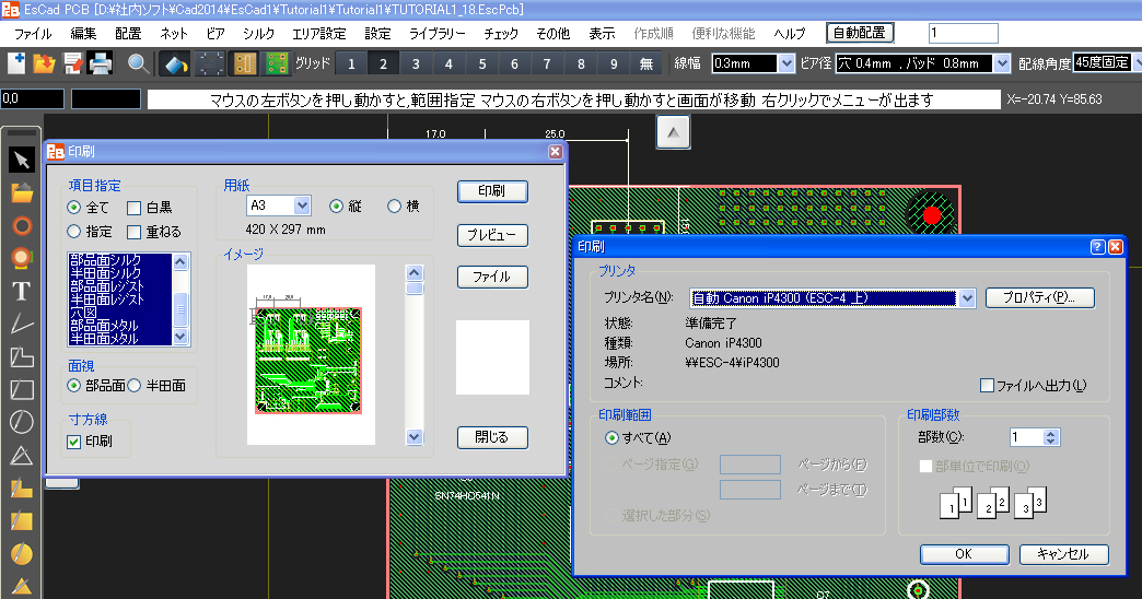
The Board Diagram is going to be printed out as follows.
Select menu [File]->[Print].
The following [Print] window appears.
Because the printed size is scaled automatically, the diagram figure does not stick out of the sheet.
Now, set checked on [B/W] in the frame [Specify Item]
Also, set checked on [Print] in the frame [Dim Line].
Set the sheet size then press the button [Print].
Then the print window of the standard Windows system appears and the printout is going to be done according to its condition.
第14章 ガーバーファイルの作成
Chapter 14. Create Gerber Data File
メニュー[ファイル]->[ガーバー作成]を選択します。
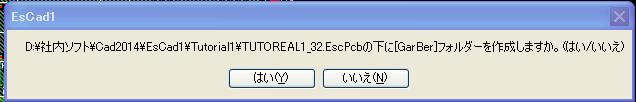
フォルダー作成を聞いてきますので、”はい”を選択します。
数秒後に、
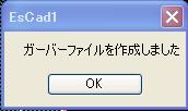
と、確認が表示されます。
ガーバーデーターは、作成したフォルダーの中に全て入っています。
Select menu [File]->[Export Gerber Data].

A message of asking folder creation appears then select "Yes".
The following message appears soon.
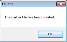
All the Gerber data files have been put in the created folder.